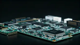

Chip-Making Revolution
ASML's new chip-making machine is a game-changer in the semiconductor industry, representing a significant advancement in the technology used to manufacture
microchips. At the heart of this machine lies EUV (Extreme Ultraviolet) lithography, a process that enables the creation of incredibly small and complex chip designs. Traditional methods struggle to achieve the precision and efficiency offered by EUV, making ASML's innovation a pivotal step forward. The EUV lithography system uses extreme ultraviolet light to 'print' circuits onto silicon wafers, a process involving highly complex mirrors and optics to ensure the light is precisely focused. This allows for smaller transistors and denser chip designs, which translates to faster and more powerful devices. This innovative approach pushes the boundaries of what is achievable in chip manufacturing, paving the way for advancements in computing, artificial intelligence, and numerous other technological fields. This technological leap forward has significant implications for global technological competitiveness, with nations striving to secure access to these advanced manufacturing capabilities to drive their innovation agendas and maintain their place in the modern technological landscape. Therefore, ASML's machine is not just an equipment; it is a catalyst for technological progress.
EUV Lithography Explained
EUV lithography, or Extreme Ultraviolet lithography, is the cornerstone of ASML's chip-making breakthrough. This process utilizes extreme ultraviolet light with a wavelength of 13.5 nanometers, which allows for the creation of incredibly detailed and minuscule chip designs. The light is generated by vaporizing tin droplets using a laser, creating a plasma that emits the EUV light. This light is then carefully guided and focused using a series of specialized mirrors, since conventional lenses are not effective at these wavelengths. The precision of the mirrors is crucial, as any imperfections could distort the image being 'printed' onto the silicon wafer. The process is extremely intricate, requiring a controlled environment to prevent even microscopic particles from interfering. This precise process allows chip manufacturers to create features as small as a few nanometers, which has helped to significantly boost the computing power of the next generation of electronics. EUV lithography is thus a vital component in modern chip manufacturing, enabling the creation of advanced processors, memory chips, and other components.
India's Semiconductor Aspirations
India is aiming to become a major player in semiconductor manufacturing and design. The nation's aim is to foster a local ecosystem that can compete internationally. India's government has introduced various policies and incentives to attract investments and encourage domestic manufacturing, including financial assistance and infrastructure development. The country is also focusing on workforce development, through specialized training programs and educational initiatives to create a talent pool equipped with the necessary skills for the semiconductor industry. Partnerships with international companies and collaborations with research institutions are also instrumental in technology transfer and accelerating the growth of the semiconductor sector in India. These efforts aim to reduce dependence on imports, create jobs, and establish India as a key node in the global semiconductor supply chain. By investing in the required infrastructure and skills, India is setting its sights on establishing itself in the semiconductor landscape.
India-EU FTA's Impact
The potential India-EU Free Trade Agreement (FTA) has the potential to significantly impact the semiconductor and AI sectors in India. The FTA could reduce tariffs and trade barriers, making it easier and more cost-effective for Indian companies to export semiconductors and related products to Europe, and vice versa. It also promotes investment, leading to technology transfer and collaborations, which will benefit both sides. The partnership can boost innovation and competitiveness by making it easier for companies to access resources, technology, and expertise from the EU, fostering new opportunities for AI applications and chip design. Through this agreement, the Indian and European markets become more integrated. Therefore, the FTA could play a crucial role in the growth and development of India's semiconductor and AI industries, promoting innovation, creating economic opportunities, and strengthening strategic ties between India and the EU.
Fabrication Process Unveiled
The fabrication of semiconductors is a complex process. It starts with a silicon wafer, a thin disc of silicon that serves as the foundation for the microchip. This wafer undergoes a series of steps, including cleaning, etching, and layering to create the intricate circuits and transistors. Photolithography is a vital stage, where patterns are transferred onto the wafer using light. This process is very similar to how photographs are developed. The wafer is coated with a photosensitive material, and a mask with the desired circuit pattern is placed over the wafer. The wafer is then exposed to light, which hardens the photosensitive material in the exposed areas. The unexposed areas are then etched away, leaving behind the desired pattern. This process is repeated multiple times, with each layer building upon the previous ones to create a complex three-dimensional structure. Once the circuits are formed, the wafer is cut into individual chips, which are then packaged and tested before being used in electronic devices. The process requires extreme precision and a clean environment to ensure that the chips function correctly.