


The Shrinking Frontier
The relentless pursuit of smaller, more powerful silicon is a hallmark of the tech industry, with leading companies often at the forefront of these advancements.
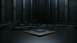
Currently, the semiconductor world is transitioning into the 2nm era, but the horizon already reveals even more ambitious goals. Reports indicate that a significant chip manufacturer is setting its sights on achieving sub-1nm chip capabilities, with trial production potentially commencing as early as 2029. This development signifies a monumental step forward in transistor density and overall processing power for the devices we rely on daily, hinting at a future where computing capabilities within our smartphones and laptops will be dramatically enhanced.
A Phased Roadmap
The journey to sub-1nm chip technology isn't envisioned as a singular, abrupt leap. Following the successful initiation of mass production for 2nm chips in late 2028, the next logical progression involves a series of refined nodes. The immediate target for this advanced foundry is the 1.4nm node, slated for deployment in 2029. This intermediate step is anticipated to yield substantial improvements, offering approximately 15 percent enhanced performance and a remarkable 30 percent boost in power efficiency. Subsequently, the focus will shift to the sub-1nm process itself, with dedicated facilities, including the Tainan A10 site and the P1-P4 plants, being prepared for this monumental transition. Initial projections for the trial phase in 2029 suggest a capacity of around 5,000 wafers per month, paving the way for devices in the early 2030s equipped with unparalleled transistor density.
Driving Next-Gen Computing
The push towards sub-1nm fabrication is far more than a marketing ploy; it's a fundamental necessity driven by the escalating demands of modern computing, particularly with the rise of advanced artificial intelligence and increasingly complex on-device applications. As software becomes more sophisticated and AI capabilities expand, the need for robust processing power grows exponentially. These advanced chip nodes are crucial for meeting these expanding performance requirements without unduly compromising battery life, ensuring that devices remain both powerful and practical for everyday use. The ability to pack more transistors into smaller spaces is key to enabling the next wave of innovation in computing.
Challenges Ahead
Despite the exciting prospect of sub-1nm chips, the path forward is not without its hurdles. Manufacturing yields, which remain a persistent challenge even with current 2nm processes, are expected to continue to be a significant factor. The intricate nature of producing these cutting-edge semiconductor components means that costs will likely remain substantial. Consequently, it is anticipated that devices featuring these ultra-advanced SoCs will initially be exclusive to the highest-tier flagship models for the foreseeable future. While the physical size of the chips may shrink, the financial investment required for these premium devices is projected to trend upwards, reflecting the immense engineering and manufacturing efforts involved.