


A Funding Breakthrough
A significant leap forward in semiconductor innovation has been marked by the successful funding round of $40 million for Lace, a forward-thinking startup.
This substantial capital infusion is earmarked to accelerate the development of their next-generation chipmaking equipment. The company, notably supported by Microsoft, is on a mission to fundamentally transform the way semiconductors are produced. While the exact technical blueprints remain proprietary, the sheer scale of this investment underscores the profound potential and industry anticipation surrounding Lace's disruptive approach to microchip fabrication.
Helium Beams: The Future
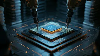
At the heart of Lace's revolutionary vision lies a novel application of helium atom beams for etching circuits onto semiconductor wafers. This technique offers a dramatic improvement over current industry standards, such as extreme ultraviolet (EUV) lithography, which is predominantly utilized by major players like ASML. Experts suggest that this helium-based method could enable the creation of chip designs that are up to ten times smaller than what is currently achievable. This opens up unprecedented possibilities for crafting incredibly dense and powerful microprocessors, potentially reshaping the landscape of high-performance computing and artificial intelligence.
Atomic Precision Unlocked
The core advantage of employing helium atom beams, as highlighted by industry specialists, is the unprecedented ability to miniaturize features such as transistors – the fundamental building blocks of all modern chips. This technology promises to etch these components to an order of magnitude smaller, reaching a scale that was previously considered almost unimaginable. This breakthrough is particularly crucial as the semiconductor industry faces the physical limitations of Moore's Law, which has long predicted the doubling of transistors on a chip roughly every two years. Lace's innovation could provide a vital pathway to continue this exponential growth in chip density and performance.
Transforming Computing Power
The implications of Lace's advancements are far-reaching, particularly for the burgeoning fields of artificial intelligence and cloud computing. By enabling the creation of smaller and more densely packed chips, the technology is expected to significantly enhance the processing power of AI accelerators, streamline the infrastructure for cloud services, and pave the way for a new generation of sophisticated electronic devices. Lace has set a target to deliver a pilot testing tool by 2029, with a full commercial rollout anticipated in the early 2030s, contingent upon successful scaling and widespread industry adoption, marking a pivotal moment in technological evolution.
Strategic Investment and Supply Chain
The substantial backing from Microsoft underscores the strategic imperative for securing the future of chip manufacturing, especially given the increasing demand for advanced computing power, particularly in AI development. Analysts also foresee Lace's success as a potential catalyst for reshaping the global semiconductor supply chain. Such a development could lessen the reliance on existing dominant manufacturers, fostering greater diversity and resilience in chip production capabilities worldwide, thereby ensuring a more robust and competitive industry ecosystem for the future.