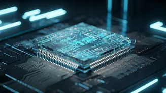


Pioneering 3D Chip Technology
India is making a significant stride in the global semiconductor industry by establishing its inaugural advanced 3D chip packaging unit in Bhubaneswar.
This ambitious project is a cornerstone of the India Semiconductor Mission, designed to cultivate a comprehensive domestic chip ecosystem. The collaboration involves key international players, including US-based 3D Glass Solutions, Intel, and Lockheed Martin, alongside other investors, signaling a robust commitment to advancing the nation's technological capabilities. This initiative represents a pivotal moment, potentially enabling India to move beyond mere assembly and towards the sophisticated manufacturing of cutting-edge semiconductor components. The project's potential for a revised, significantly larger budget underscores the scale of investment and the high expectations for its success in placing India on the map for advanced chip production.
Strategic Importance & Vision
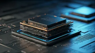
The development of this 3D chip packaging unit is strategically crucial for India's aspiration to achieve self-sufficiency in semiconductor manufacturing. The India Semiconductor Mission aims to create a complete end-to-end ecosystem, reducing reliance on foreign imports and fostering innovation. Advanced 3D packaging allows for the stacking of multiple chip components vertically, leading to more powerful, smaller, and energy-efficient devices. This capability is vital for next-generation technologies, including artificial intelligence, 5G, and advanced computing. By investing in such cutting-edge infrastructure, India positions itself as a key player in the global supply chain for advanced semiconductors, offering significant economic and technological advantages.
Technological Leap Forward
This new facility represents a substantial technological leap for India. Traditional 2D chip manufacturing involves placing components side-by-side on a silicon wafer. In contrast, 3D chip packaging involves intricate techniques to stack chips and interconnect them vertically. This allows for greater processing power and reduced physical footprint, essential for the miniaturization trend in electronics. The project's involvement with leading tech giants ensures access to the latest manufacturing processes and quality standards. This not only bolsters India's manufacturing prowess but also cultivates a highly skilled workforce capable of operating and innovating within this advanced technological domain, setting a new benchmark for the country's industrial capabilities.