


Pioneering 3D Chip Technology
India's semiconductor landscape is set for a transformative upgrade with the commencement of its inaugural advanced 3D chip packaging plant in Bhubaneswar,
Odisha. This pioneering facility is being brought to life by the expertise of US-based 3D Glass Solutions Inc, operating through its wholly owned Indian subsidiary, Heterogeneous Integration Packaging Solutions Pvt Ltd. The initiative has garnered significant financial backing from prominent entities, including Intel, whose CEO, Lip-Bu Tan, participated virtually in the foundational ceremony. This marks a pivotal moment, propelling India into a new phase of high-tech manufacturing and innovation within the critical semiconductor sector.
Economic and Employment Boost
The establishment of this cutting-edge facility represents a substantial investment in Odisha's economic future. The project, which received approval under the India Semiconductor Mission (ISM) with a proposal valued at Rs 1,934 crore, is projected to achieve remarkable production capacities. It is anticipated to manufacture 70,000 specialized glass panels annually, alongside 50 million assembled units. Furthermore, the plant is expected to produce approximately 13,000 advanced 3DHI modules, underscoring its advanced technological capabilities. Critically, this venture is poised to generate an estimated 2,500 direct and indirect employment opportunities, significantly contributing to local job creation and economic development within the state.
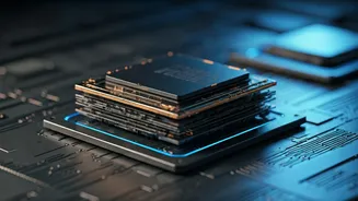
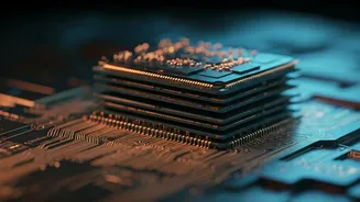
Advancing Semiconductor Capabilities
The core of this new facility lies in its utilization of advanced 3D glass semiconductor technology. This sophisticated process employs specialized glass substrates, which are instrumental in enabling high-performance, three-dimensional integration of intricate electrical components. The advantages of using glass over traditional silicon are considerable; it offers superior radio frequency performance, markedly lower electrical losses, and enhanced thermal stability, particularly beneficial for integrating passive components. The plant's operational focus will be on the assembly and packaging of these highly advanced chips, thereby bolstering India's capabilities in the global semiconductor supply chain.
Shifting Industrial Focus
The groundbreaking ceremony was hailed as a watershed moment for Odisha, signifying a strategic diversification of its industrial base. For decades, the state has been predominantly known for its strength in sectors like mining, metals, and power generation. However, the inauguration of this high-tech semiconductor plant signals a decisive pivot towards embracing advanced industries. This move is expected to position Odisha as a burgeoning hub for information technology and electronics manufacturing, aligning with national goals for technological self-reliance and manufacturing excellence. It represents a forward-looking approach to economic development, harnessing cutting-edge technology to drive future growth.