


New Tech Hub Unveiled
On February 28th, Prime Minister Narendra Modi marked a significant milestone for India by inaugurating the country's first semiconductor fabrication facility.
Located in Sanand, this state-of-the-art Assembly, Testing, Marking, and Packaging (ATMP) plant is a joint venture with Micron Technology, Inc., representing an investment exceeding Rs. 20,000 crore, specifically Rs. 22,516 crore. The facility is designed to bolster India's capabilities in producing advanced semiconductor components, particularly for DRAM and NAND flash memory products, as well as Solid State Drive (SSD) storage devices. This venture is poised to address a growing demand for these critical tech elements, not only within India but also across international markets. The inauguration was preceded by a roadshow in Sanand, highlighting the national importance of this technological advancement. The establishment of this plant signifies India's ambitious stride towards self-reliance in the high-tech semiconductor industry, a sector crucial for numerous modern technologies and economic growth.
Job Creation and Inclusivity
Beyond its technological prowess, the new Sanand facility is a significant catalyst for employment and economic opportunity. The plant is currently employing 2,000 individuals, with projections to expand this workforce to 5,000 direct job opportunities in the future. A notable aspect of their hiring strategy, as highlighted by the state government, is the active inclusion of Divyang (specially-abled) citizens who are serving as operators and technicians. This demonstrates a commitment to fostering an inclusive work environment, providing meaningful careers to skilled individuals from all walks of society. This focus on creating diverse employment avenues underscores the broader impact of such large-scale industrial projects, contributing not just to economic output but also to social development and equitable opportunity within the region and beyond.
Memory, Storage, and AI
The strategic importance of this facility is deeply intertwined with the evolution of technology, particularly the burgeoning field of Artificial Intelligence (AI). Sanjay Mehrotra, the Chairman, President, and CEO of Micron Technology, emphasized that memory and storage are fundamental pillars of modern technological infrastructure, especially for AI systems. He explained that AI applications depend critically on robust memory and storage capabilities to function at peak efficiency. As AI continues to advance, enabling faster and real-time processing, the requirement for more sophisticated and high-performance memory solutions is escalating rapidly. This Sanand plant, by producing advanced DRAM and NAND wafers and converting them into finished memory products, is directly positioned to support this escalating global demand driven by AI advancements and other data-intensive applications, ensuring India plays a pivotal role in this technological frontier.
Phased Expansion Plans
Micron Technology's strategic vision for its Sanand operations unfolds in distinct phases, reflecting a long-term commitment to growth and development. The company initially disclosed its intention to establish a new assembly and test facility in Gujarat in June 2023. Phase I of this ambitious project involves the development of approximately 500,000 square feet of dedicated cleanroom space, a critical component for semiconductor manufacturing. Looking ahead, the company, which is headquartered in Boise, Idaho, has outlined plans for Phase 2. This subsequent phase is projected to involve the construction of a facility comparable in scale to the initial phase and is expected to commence in the latter half of the current decade. Such a phased approach allows for meticulous planning, technological integration, and a sustainable ramp-up of production capacity, ensuring the facility can adapt to evolving market needs and technological advancements.
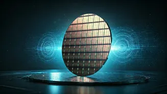
ATMP Plant's Functionality
Understanding the operational flow of an ATMP plant is key to appreciating the complexity and sophistication of semiconductor manufacturing. The new facility in Sanand will focus on transforming raw wafers into finished, functional components such as ball grid array (BGA) integrated circuit packages, memory modules, and SSD devices. The entire semiconductor journey begins with silicon, extracted from sand, melted, and formed into cylindrical ingots. These ingots are then sliced into extremely thin discs called wafers. In the fabrication plant, intricate electronic patterns are imprinted onto these wafers using processes like photolithography, where multiple layers are precisely applied to create transistors that form the memory circuits. Once these chips are created and cut from the wafers, they arrive at the ATMP plant for the critical assembly and testing stages. Here, they are rigorously checked for performance metrics like speed and capacity. Following successful testing, the chips are marked with identifying information and then packaged, ready for deployment in global markets, particularly for high-demand sectors like AI.
Sanand's Expanding Infrastructure
In tandem with the advancements in the semiconductor industry, the Sanand Industrial Estate is also witnessing significant development in its supporting infrastructure. To better accommodate the needs of the numerous national and multinational corporations operating within the estate, a substantial plot of land measuring 20,168.54 square meters, approximately 5 acres, in the Sanand-2 Industrial Estate has been earmarked for the construction of a premium hotel. The e-auction for this strategically located plot concluded on December 22, 2025. The developer has been granted a four-year period to commence the construction of a 3 to 5-star hotel. This development is particularly timely, as a five-star hotel is already under construction nearby. The upcoming hotel is expected to serve as a convenient accommodation option for visiting delegates, international business partners, and employees of the multinational companies establishing a presence in the region, especially with the inauguration of the advanced semiconductor plant.