






What's Happening?
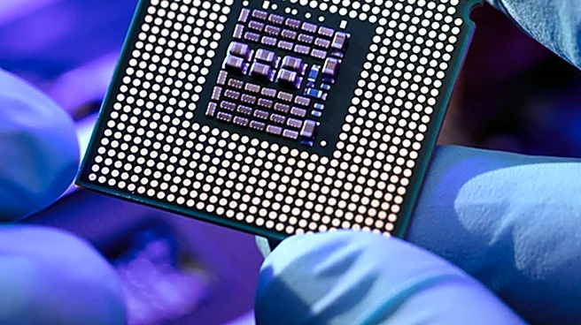
Researchers from Kyoto University have successfully fabricated heat-resistant silicon carbide (SiC) transistors on 6-inch wafers, marking a significant step towards practical integrated circuits for extreme environments. This development builds on their
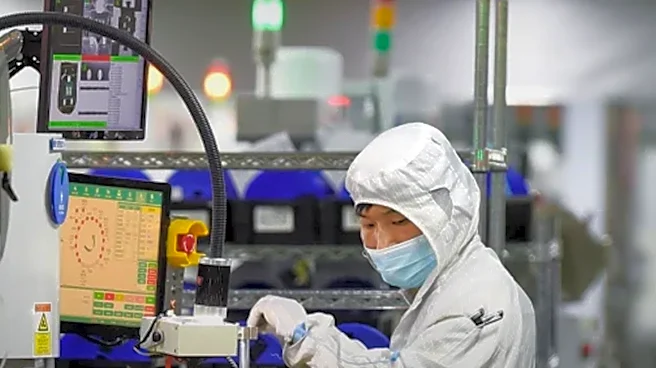
previous work with junction field-effect transistors (JFETs) and has resulted in a new SiC transistor structure capable of operating at 600°C (1,112°F). The team collaborated with Phenitec Semiconductor Corp., a mass-production fabrication plant, to achieve wafer-scale production, which is crucial for practical applications requiring a large number of very small transistors. The fabricated SiC transistor demonstrated high uniformity, with a standard deviation of its threshold voltage less than 0.07 volts in the wafer's center region, a key technical milestone for integrated circuit fabrication.
Why It's Important?
This breakthrough expands the potential applications of semiconductors into previously inaccessible areas. The ability to produce highly uniform, heat-resistant SiC transistors on a wafer scale opens doors for electronic circuits in extreme environments such as jet engine sensors, geothermal resource development, and even space exploration, like Venus. The move from laboratory-scale production to an industry-standard mass-production plant is critical for bridging the gap between academic research and real-world societal use. This advancement could lead to more robust and reliable electronics in demanding conditions, reducing the risk of failure and enabling new technological capabilities in various industries. The collaboration between academia and industry is also a significant factor, demonstrating how such partnerships can accelerate the development and practical implementation of advanced technologies.
What's Next?
The research team, led by first author Mitsuaki Kaneko, aims to establish a startup to further develop and commercialize this technology. While many challenges remain, the successful wafer-scale fabrication and high uniformity achieved in the initial trials suggest a promising path forward for integrated circuit technology in extreme environments. Future steps will likely involve further optimization of the fabrication process, continued testing to ensure long-term reliability in diverse harsh conditions, and the development of specific integrated circuit designs that leverage these new transistors. The focus will be on translating this technical milestone into commercially viable products that can withstand high temperatures and other extreme conditions, ultimately expanding the reach of electronic systems into new and critical applications.
Beyond the Headlines
The development of heat-resistant SiC transistors on 6-inch wafers represents a fundamental shift in material science and semiconductor manufacturing. Silicon carbide, with its superior thermal properties compared to traditional silicon, has long been recognized for its potential in high-power and high-temperature electronics. This achievement signifies a maturation of SiC technology, moving it from theoretical promise to practical application. The high uniformity achieved in wafer-scale production is particularly noteworthy, as it directly impacts the yield and cost-effectiveness of manufacturing integrated circuits. This could lead to a new generation of electronics that are not only more resilient but also more energy-efficient, given SiC's inherent advantages in power conversion. The implications extend beyond specific applications, potentially influencing the design and reliability standards for all electronics operating under challenging conditions, pushing the boundaries of what is currently possible with semiconductor technology.