






What's Happening?
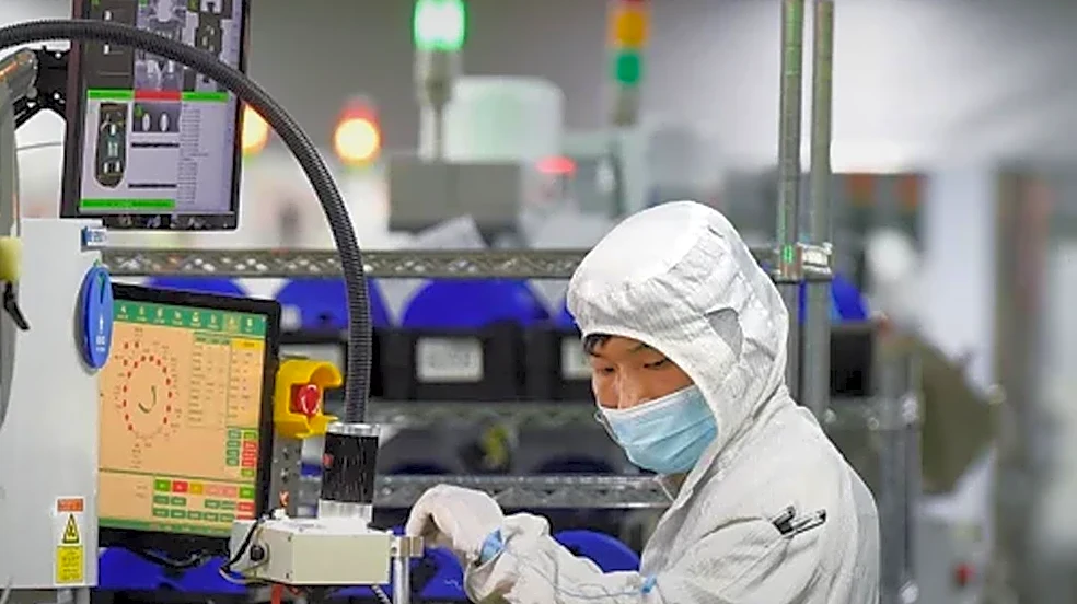
Intel has begun installing production tools at its Fab 62 in Arizona, with the facility on track for mass production by late 2028. The company also reported significant progress on its 'Ohio One' manufacturing complex, where the first major structural
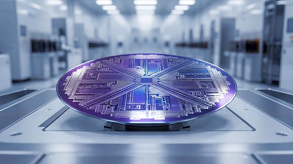
truss has been installed at the site's first semiconductor fab. Intel confirmed the integration of High-NA EUV lithography into high-volume manufacturing (HVM) for 2028, a crucial step for producing advanced chips. Intel's U.S. operations involve over 4,500 suppliers across 49 states, with annual domestic expenditures exceeding $29 billion. The company emphasizes that domestic semiconductor leadership requires not only wafer fabrication capacity but also research, process development, advanced packaging, and a comprehensive supply chain.
Why It's Important?
These developments are vital for strengthening the U.S. domestic semiconductor industry and reducing reliance on foreign manufacturing. The installation of production tools at Fab 62 and the progress at 'Ohio One' signify concrete steps towards increasing advanced chip production within the United States. The integration of High-NA EUV lithography positions Intel at the forefront of semiconductor technology, enabling the production of smaller, more powerful, and energy-efficient chips. This is crucial for various sectors, including artificial intelligence, defense, and telecommunications. Intel's extensive network of U.S. suppliers and substantial domestic expenditures highlight the broad economic impact of these investments, fostering job creation and technological innovation across multiple states. A robust domestic semiconductor ecosystem is essential for national security and economic competitiveness.
What's Next?
Intel expects Fab 62 to become operational before the end of 2028, although specific details on high-volume production start dates or the nodes to be produced are yet to be confirmed. The 'Ohio One' complex will continue its construction, with Intel aiming to expand domestic production of chips using leading-edge process technologies for years to come. Intel will also continue to invest in its leading-edge process technology R&D, advanced packaging, and photomask production capabilities in the U.S. The company's commitment to integrating High-NA EUV into HVM by 2028 indicates a clear roadmap for future technological advancements. These ongoing investments are part of Intel's long-term strategy to ensure U.S. leadership in semiconductor innovation and manufacturing.
Beyond the Headlines
Intel's strategic investments in Arizona and Ohio, coupled with the adoption of High-NA EUV technology, represent a significant push towards re-establishing the U.S. as a global leader in semiconductor manufacturing. This goes beyond mere production capacity, encompassing the entire value chain from research and development to advanced packaging. The emphasis on 'truly American-made' technologies, as highlighted by Intel, underscores the importance of domestic innovation and intellectual property. This comprehensive approach aims to create a self-sufficient semiconductor ecosystem, reducing vulnerabilities to geopolitical shifts and supply chain disruptions. The long-term implications include enhanced national security, sustained economic growth through high-tech job creation, and a strengthened position in the global technology race, particularly in emerging fields like AI and quantum computing.