








What's Happening?
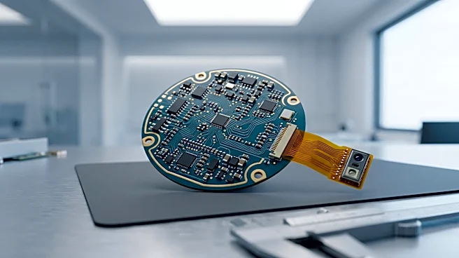
The design of Printed Circuit Boards (PCBs) for smartwatches is undergoing significant evolution to accommodate more advanced sensing and communication capabilities within compact, sealed cases. Early smartwatch designs were relatively simple, featuring
a microcontroller, accelerometer, and Bluetooth radio. Modern smartwatches now integrate complex components such as optical photoplethysmography (PPG), ECG electrodes, temperature sensors, GNSS, audio, and cellular support. This increased functionality necessitates innovative PCB structures, often combining rigid main boards with flexible circuits to connect displays, sensors, and buttons. Key design challenges include managing power paths for current peaks, precise placement of optical sensors, ensuring RF and antenna clearance, and addressing fine-pitch assembly requirements, all while preserving battery life and signal quality.
Why It's Important?
The advancements in smartwatch PCB design are critical for the continued growth and innovation of the U.S. wearables market. As consumers demand more sophisticated health monitoring, communication, and lifestyle features from their smartwatches, the underlying hardware must evolve to support these capabilities. Efficient and compact PCB designs enable manufacturers to integrate more sensors and functionalities without compromising device size or battery life. This directly impacts product competitiveness, user experience, and the potential for new applications in health, fitness, and daily life. The challenges in design also drive innovation in materials science and manufacturing processes, benefiting the broader electronics industry.
What's Next?
The future of smartwatch PCB design will likely see even greater sensor integration and more functions processed at the device's edge, further compressing available PCB area. Manufacturers will continue to focus on partitioning layouts into rigid component islands and short interconnect routes, utilizing advanced features like High-Density Interconnect (HDI) where necessary. Ongoing efforts will be directed towards separating optical and analog paths from noisy power sources, prototyping and tuning antennas with actual case and wrist loading, and developing robust solutions for flex fatigue. The industry will also prioritize making alignment marks, test points, and assembly fixtures part of the design package to ensure consistent production quality for increasingly complex devices.
Beyond the Headlines
The intricate engineering behind smartwatch PCBs reflects a broader trend in miniaturization and integration across consumer electronics. This push for more functionality in smaller form factors has implications for sustainability, as complex, tightly integrated devices can be challenging to repair or recycle. Ethical considerations arise regarding the environmental impact of manufacturing these advanced components and the lifecycle management of e-waste. Culturally, the increasing sophistication of smartwatches further embeds technology into personal health and daily routines, potentially influencing user expectations for instant data and continuous connectivity. This technological frontier also highlights the ongoing tension between design aesthetics, functional capability, and manufacturing feasibility.