






What's Happening?
E&R Engineering Corp., an international provider of semiconductor packaging equipment, is set to open a new Malaysian subsidiary, E&R SEMICONDUCTOR (MALAYSIA) SDN. BHD., at the Melaka Free Trade Zone on October 13. This strategic move aims to enhance
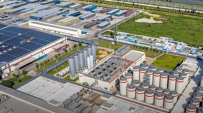
the company's global strategy for its packaging materials business unit, shifting a portion of its production focus from China to Malaysia while simultaneously expanding overall capacity. The new facility is currently undergoing sample testing and qualification, with mass production anticipated to commence early next year. This expansion is expected to generate 50 local job opportunities and bolster E&R's supply capabilities for semiconductor and OSAT customers across Southeast Asia. The company's President, KS Chen, stated that this shift addresses growing customer demand in the region and will establish the facility as a local hub for E&R's semiconductor equipment Field Service Engineers, focusing on hiring local talent to provide immediate technical support and after-sales services.
Why It's Important?
This expansion by E&R Engineering into Malaysia is significant for the global semiconductor industry, particularly in Southeast Asia. Malaysia currently accounts for approximately 13% of the world's backend packaging and testing capacity, with its semiconductor market projected to reach $16.51 billion by 2030, driven by robust policy support. E&R's localized mass production of advanced carrier tapes will shorten lead times for OSAT and semiconductor customers, providing high precision, excellent electrostatic discharge (ESD) protection, and robust packaging interfaces crucial for advanced packaging trends like chip miniaturization and Chiplet integration. This move will strengthen the supply chain for critical components in the semiconductor sector, reducing reliance on single-region production and enhancing resilience against potential disruptions. For the U.S. semiconductor industry, a more robust and diversified global supply chain, particularly in Southeast Asia, can lead to greater stability and efficiency in sourcing essential packaging materials, ultimately impacting the cost and availability of electronic components.
What's Next?
The new Malaysian facility is scheduled to begin mass production early next year, following its grand opening on October 13. E&R Engineering will focus on hiring local talent to build its specialized equipment engineering team, ensuring localized technical support and after-sales services. The company's General Manager of the Malaysia plant, AK Ong, emphasized a commitment to delivering top-quality products and strict quality monitoring. This expansion is expected to further integrate E&R into Southeast Asia's packaging hub, potentially leading to increased collaboration with regional semiconductor manufacturers and OSAT providers. The success of this new plant could influence future investment decisions by other global semiconductor suppliers looking to diversify their manufacturing footprint and capitalize on the growing demand in the region. The company will likely monitor the market response and operational efficiency of the new plant to inform subsequent strategic developments.
Beyond the Headlines
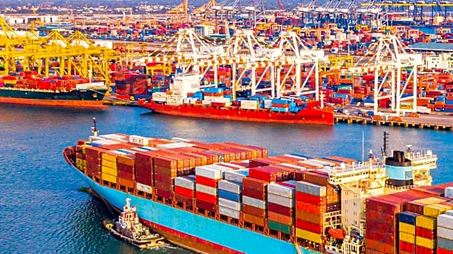
The strategic shift of E&R Engineering's production to Malaysia highlights a broader trend in the technology sector towards diversifying manufacturing bases, particularly in response to geopolitical considerations and the desire for more resilient supply chains. This move not only addresses immediate market demands but also positions the company to mitigate risks associated with concentrating production in a single country. The emphasis on localized manufacturing and services, including hiring local talent and providing immediate technical support, reflects a growing understanding of the importance of regional integration and responsiveness in complex global industries. This approach can foster stronger local economies and create a more interconnected, yet distributed, global manufacturing ecosystem. The long-term implications could include a more competitive and innovative semiconductor packaging landscape, with increased regional specialization and enhanced capabilities to support the rapid evolution of semiconductor technology.