





What's Happening?
The electronics industry is facing new engineering challenges driven by increasing complexity, miniaturization, and supply chain disruptions. As electronic components become more powerful and compact, issues such as thermal management, obsolescence of
parts, and the need for rapid product development are becoming critical. Advanced manufacturing and packaging technologies, including 2.5D and 3D integration and chiplets, enable greater functionality in smaller spaces but also create new demands for precise physical geometry characterization. Supply chain disruptions, exacerbated by the surge in demand for AI-related hardware, lead to production bottlenecks and the need for alternate sourcing, where replacement components may be functionally equivalent but physically different. 3D scanning and reverse engineering are emerging as crucial tools to address these challenges by accurately capturing the physical geometry of components and assemblies.
Why It's Important?
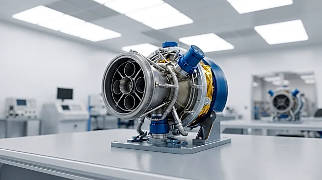
The application of 3D scanning in electronics manufacturing is vital for U.S. industries, particularly in maintaining operational continuity and fostering innovation. For manufacturers dealing with obsolete equipment, 3D scanning allows for the reproduction of unavailable parts, preventing costly production shutdowns. This capability is especially important in sectors reliant on legacy systems, ensuring that critical infrastructure and manufacturing processes remain functional. In advanced semiconductor packaging, where precise physical relationships are paramount, 3D scanning provides the accuracy needed to characterize complex structures, ensuring proper alignment, surface quality, and mechanical fit. This directly impacts the performance and reliability of high-tech products, from consumer electronics to defense systems. Furthermore, in the face of supply chain vulnerabilities, 3D scanning enables companies to quickly develop alternate sourcing strategies by capturing the geometry of existing parts and converting it into digital design files, reducing dependence on disrupted suppliers and enhancing supply chain resilience for U.S. businesses.
What's Next?
The adoption of 3D scanning technology is expected to grow as electronics continue to evolve and engineering challenges intensify. Manufacturers will increasingly integrate 3D scanning into their design, production, and maintenance workflows to manage complexity and accelerate product development cycles. The technology will become more sophisticated, offering faster data capture and higher accuracy, further shortening the path from physical component to usable engineering data. Collaboration between 3D scanning solution providers and electronics manufacturers will likely expand to address specific industry needs, such as characterizing advanced cooling systems and ensuring compatibility in heterogeneous integration. As the industry pushes towards even greater miniaturization and higher power densities, the ability to accurately understand and reproduce physical components will be a competitive differentiator, driving further investment in advanced metrology solutions.
Beyond the Headlines
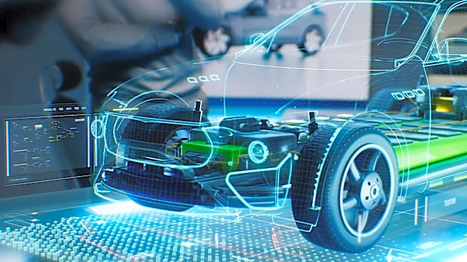
The increasing reliance on 3D scanning in the electronics industry points to a deeper philosophical shift in engineering: the convergence of the physical and digital worlds. As products become more intricate, the distinction between 'as-designed' (CAD models) and 'as-built' (physical parts) becomes critical. 3D scanning bridges this gap, providing a digital twin of physical reality that can be analyzed, modified, and reproduced with unprecedented precision. This capability has ethical implications regarding intellectual property, as reverse engineering becomes more accessible. It also highlights the importance of data management and cybersecurity for these highly detailed digital models. Culturally, it signifies a move towards more agile and adaptive manufacturing processes, where physical constraints can be rapidly understood and overcome, fostering a culture of continuous improvement and resilience in the face of technological and logistical hurdles. This integration of advanced metrology is not just about solving problems but about fundamentally changing how we approach design and production in the digital age.