





What's Happening?
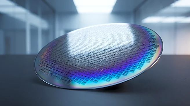
Intel has confirmed its commitment to ASML's High Numerical Aperture (High NA) Extreme Ultraviolet (EUV) lithography systems, announcing that the technology is already being used in high-volume manufacturing. Intel Foundry and ASML reported that over
one million wafers have been processed using High NA tools for early certification, testing, research and development, and volume production of selected layers for Intel Core Ultra Series 3 processors, code-named Panther Lake. Intel stated that the overlay, throughput, and availability of these High NA systems are meeting expectations, with performance matching or exceeding comparable layers produced using ASML's existing NXE EUV platform. This adoption signals a significant step for the semiconductor industry, as High NA EUV machines, costing approximately $400 million each, are twice as expensive as current EUV systems but are crucial for printing smaller features and potentially reducing manufacturing steps for advanced chips.
Why It's Important?
Intel's early and successful adoption of High NA EUV technology is a critical validation for the next generation of chipmaking. This move suggests that the substantial investments driven by the artificial intelligence boom are pushing highly expensive and consequential semiconductor technologies from experimental stages into broader production. High NA is not merely an incremental upgrade but a fundamental advancement designed to enable the creation of more powerful and efficient chips, which are essential for AI and other demanding applications. This commitment from Intel, a leading chipmaker, could accelerate the wider industry adoption of High NA, influencing other major players like TSMC, Samsung, SK Hynix, and Micron, who have also made commitments or ordered these machines. The successful integration of High NA could solidify ASML's monopoly in leading-edge lithography and further extend its technological advantage, shaping the competitive landscape of the global semiconductor market for years to come.
What's Next?
The successful deployment of High NA EUV by Intel is expected to pave the way for broader industry adoption. Other major chipmakers, including Samsung and SK Hynix, plan to begin memory-chip production using High NA in 2028, while TSMC has committed to using the technology from 2030. The industry will continue to work on standardizing and evolving the surrounding ecosystem, including masks, software, materials, and automation processes, to fully leverage High NA capabilities. Intel is actively championing the adoption of larger 6-by-12-inch masks to optimize High NA scaling. The ongoing AI-driven investment cycle is a key factor in the continued demand for these advanced machines, and ASML's CEO believes the AI boom is far from over. Future developments will likely focus on optimizing the cost-effectiveness and efficiency of High NA systems to meet the escalating demands for advanced computing power.
Beyond the Headlines
The embrace of High NA EUV technology by Intel and other industry leaders highlights a profound shift in the economics of chip manufacturing, driven largely by the insatiable demands of artificial intelligence. The willingness to invest hundreds of millions of dollars per machine underscores the strategic imperative for chipmakers to push the boundaries of miniaturization and performance. This development also points to the immense collaborative effort required across the semiconductor ecosystem, involving equipment manufacturers, mask makers, software providers, and materials suppliers, to bring such complex technology to fruition. The long-term implications include not only faster and more powerful devices but also potential shifts in global technological leadership, as nations and companies vie for supremacy in advanced chip production. The ethical considerations around the environmental impact of such energy-intensive manufacturing processes and the geopolitical implications of concentrated technological power will also become increasingly relevant.