







What's Happening?
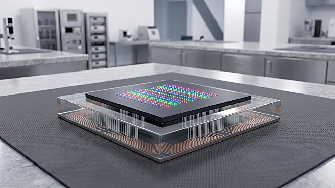
Intel has secured a U.S. patent detailing the embedding of MicroLEDs directly into chip packaging, specifically within a glass substrate. This innovative design connects semiconductor dies equipped with MicroLEDs via Through-Glass-Vias (TGV) to supply
power and signal, enabling them to emit red, green, and blue (RGB) light. Intel suggests this technology could serve multiple purposes, including diagnostic testing by providing visual indicators of completed tests or failures without external LEDs. Additionally, it could be used for aesthetic personalization, allowing for illuminated lettering on the chip's surface for DIY electronics. The patent also hints at the potential for this technology to support optical signaling, aligning with ongoing developments in co-packaged optics (CPO) for high-speed interconnects, particularly in AI data centers.
Why It's Important?
This patent signifies a crucial step in Intel's long-term investment in glass substrate technology and advanced chip packaging, with significant implications for the U.S. semiconductor industry. The integration of MicroLEDs directly into chip packages could revolutionize diagnostic processes, making chip validation and testing more streamlined and efficient, thereby reducing manufacturing costs and accelerating product development cycles. More profoundly, the potential for optical interconnects through this technology could address the escalating demand for higher bandwidth and lower energy consumption in data centers, especially with the rapid growth of AI. This could give Intel a competitive edge in the high-performance computing market, impacting the design and efficiency of future AI infrastructure and potentially influencing the broader U.S. technology landscape by enabling faster and more energy-efficient data transfer within and between chips.
What's Next?
Intel's next steps will likely involve further research and development to transition this patented technology from concept to practical application. This includes refining the manufacturing processes for embedding MicroLEDs in glass substrates and developing the necessary optical fiber solutions and receivers to create a full optical interconnect module. Collaboration with companies like AU Optronics, which is also developing Micro LED CPO modules, could accelerate Intel's progress in this area. Industry stakeholders, including other semiconductor manufacturers and data center operators, will closely monitor Intel's advancements, potentially leading to increased investment in similar in-package optical technologies. The development could also influence future industry standards for chip packaging and interconnects, pushing towards more integrated and optically-driven solutions.
Beyond the Headlines
Beyond the immediate technical benefits, Intel's patent reflects a deeper trend in the semiconductor industry towards holistic chip design, where packaging is no longer just a protective shell but an integral part of the chip's functionality. The aesthetic application of in-package LEDs, while seemingly minor, could foster a new culture of personalization in electronics, blurring the lines between functionality and design in consumer and enthusiast markets. More critically, the potential for optical interconnects addresses fundamental limitations of electrical signaling, such as power consumption and bandwidth, which are becoming bottlenecks for advanced computing. This shift towards optical communication within chips could trigger a paradigm change in how computing architectures are designed, potentially leading to entirely new classes of high-performance, energy-efficient devices and systems, with profound long-term implications for technological innovation and sustainability.