




What's Happening?
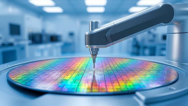
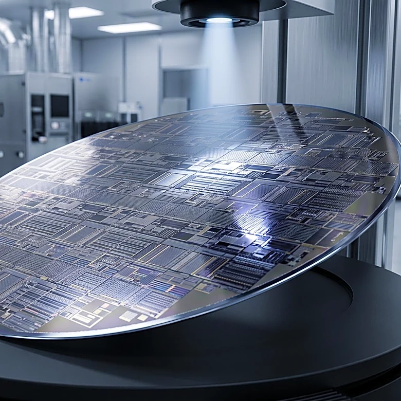
SUSS MicroTec SE, a prominent supplier of equipment and process solutions for the semiconductor industry, has announced its entry into the wafer-level cleaning market. This expansion is marked by the launch of its new GreenTec Solutions product line and the introduction
of its first system, the GT200. The move aims to capitalize on the growing demand for advanced packaging, heterogeneous integration, and increasing semiconductor needs driven by AI and high-performance computing applications, which currently represent an addressable market of approximately €5.4 billion. The GreenTec Solutions portfolio features a hybrid cleaning approach that combines SUSS's established TurbulenStrip™ and CrustBuster™ process technologies. These technologies are designed to offer efficient resist and residue removal, along with the breakdown of organic materials, while significantly reducing chemical consumption and eliminating hazardous acids, thereby supporting sustainability goals and lowering operational costs.
Why It's Important?
This strategic entry by SUSS MicroTec into the wafer-cleaning market is significant for the U.S. semiconductor industry and its global supply chain. As semiconductor manufacturing becomes more complex with advanced packaging and heterogeneous integration, efficient and sustainable wafer cleaning processes are critical for yield and performance. The GreenTec Solutions' focus on reduced chemical consumption and the elimination of hazardous acids aligns with increasing environmental, social, and governance (ESG) demands within the industry. This not only offers cost benefits to manufacturers but also addresses growing regulatory pressures and corporate sustainability objectives. The GT200, designed for 200 mm manufacturing environments in MEMS, RF, Power Device, and CMOS applications, will support the development and production of next-generation microchips essential for AI and high-performance computing, areas where the U.S. is a major player.
What's Next?
The GT200 is currently designed for research and development, process qualification, and production in 200 mm manufacturing environments. SUSS MicroTec has outlined a clear roadmap for its GreenTec Solutions product line, emphasizing modularization and standardization. The company plans to expand its portfolio towards high-volume manufacturing (HVM) with a dedicated 300 mm HVM platform in 2027, followed by a 200 mm HVM platform in 2028. This phased approach provides customers with a clear migration path from evaluation to full-scale production. SUSS will also continue to support customers through joint evaluation programs, process co-development, and recipe optimization services to accelerate adoption and improve process stability. The strong customer interest has prompted SUSS to expedite the launch of the 300 mm HVM solution, indicating a rapid market response and demand for these sustainable cleaning technologies.
Beyond the Headlines
SUSS MicroTec's entry into the wafer-cleaning market with an emphasis on 'GreenTec Solutions' highlights a broader industry trend towards sustainable manufacturing practices in the semiconductor sector. Beyond the immediate economic and technological benefits, this move reflects a growing awareness and commitment to environmental responsibility within high-tech industries. The reduction of hazardous chemicals and waste generation in wafer fabrication processes has long-term implications for environmental protection and worker safety. This shift could also influence supply chain dynamics, favoring suppliers who can offer eco-friendly solutions. Culturally, it reinforces the idea that technological advancement and environmental stewardship are not mutually exclusive but can be integrated for mutual benefit. The success of such initiatives could set new industry standards, encouraging other manufacturers to adopt similar sustainable practices and contributing to a more responsible global technology ecosystem.