





What's Happening?
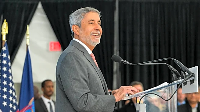
SK Hynix, a leading South Korean memory chip maker, has ceremonially broken ground on its new advanced packaging facility in West Lafayette, Indiana. Indiana Governor Mike Braun, SK Hynix CEO Kwak Noh-Jung, and other officials attended the event, marking
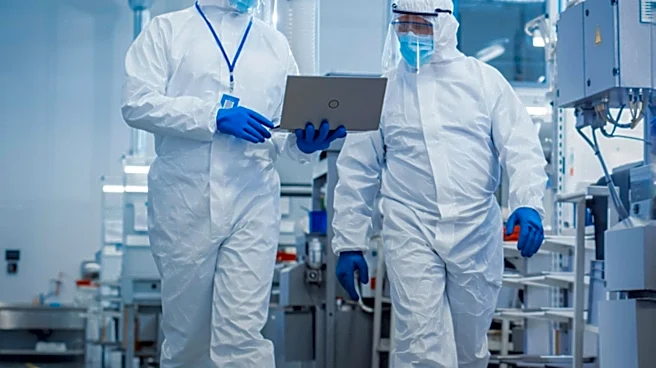
a significant $4 billion investment. This facility is projected to create approximately 1,000 direct jobs and an additional 6,000 jobs through construction and business partnerships. The factory will focus on packaging high-bandwidth memory (HBM) chips, which are crucial for artificial intelligence applications and are currently in high demand globally. While the chips themselves will be manufactured in South Korea and China, the Indiana facility will handle the critical process of stacking and connecting these memory chips. The first cleanroom is slated to open in October 2028. This project is supported by up to $458 million from the federal CHIPS Act and a state incentive package worth up to $712 million, the second largest in Indiana's history.
Why It's Important?
This investment by SK Hynix is a pivotal step in strengthening the U.S. semiconductor supply chain and reducing reliance on overseas manufacturing for advanced chip components. The facility will make Indiana a key HBM production base in America by 2030, addressing the critical global shortage of high-bandwidth memory essential for the burgeoning artificial intelligence industry. By bringing advanced packaging capabilities to the U.S., the project enhances national and economic security, as highlighted by Indiana State Senator Todd Young. The creation of 7,000 direct and indirect jobs will significantly boost Indiana's economy, providing high-wage opportunities and fostering a skilled workforce, including potential recruitment from Purdue University. This development aligns with broader U.S. efforts to onshore semiconductor production, ensuring a more resilient and secure domestic supply of vital technology.
What's Next?
Construction of the facility began in April, with the first cleanroom expected to be operational by October 2028. SK Hynix plans to initially bring employees from South Korea for the project's early stages but intends to fill long-term roles with U.S. employees, including graduates from Purdue University. The 133-acre site will also include research and development centers, allowing top AI customers to collaborate with SK Hynix on developing next-generation memory chips. SK Hynix CEO Kwak Noh-Jung indicated that the company is open to further U.S. investments and cooperation, potentially including front-end chip fabs, depending on suitable opportunities. The company's total U.S. investments and assets are projected to exceed $45 billion by 2030, signaling a long-term commitment to expanding its presence in the American semiconductor landscape.
Beyond the Headlines
The SK Hynix investment underscores the strategic importance of advanced packaging in the semiconductor industry, often overlooked in favor of front-end manufacturing. As chip designs become more complex, packaging plays an increasingly critical role in performance and efficiency, especially for AI applications. This development also highlights the effectiveness of government incentives, such as the CHIPS Act, in attracting foreign direct investment and stimulating domestic high-tech manufacturing. The collaboration between industry, state government, and academic institutions like Purdue University exemplifies a comprehensive approach to workforce development and technological innovation. This project could set a precedent for future investments in specialized semiconductor processes, fostering a more diversified and robust U.S. chip ecosystem beyond traditional fabrication plants, and addressing the intricate challenges of global supply chain vulnerabilities.