







What's Happening?
Senators Ruben Gallego (D-AZ) and Mark Kelly (D-AZ), alongside Representatives Greg Stanton (AZ-04) and Yassamin Ansari (AZ-03), have announced a federal investment of $2,062,000 for Arizona State University (ASU). This funding, awarded through the National
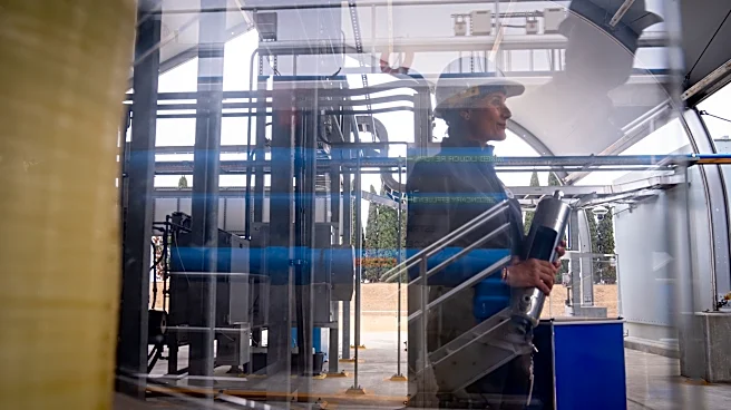
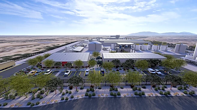
Institute of Standards and Technology (NIST) as congressionally directed spending, is designated for the development, testing, and demonstration of innovative water reuse technologies specifically for semiconductor manufacturing. The project aims to advance promising water treatment technologies from early-stage research to commercial readiness. This will involve integrating these technologies into a mobile, pilot-scale demonstration testbed and validating them under manufacturing-representative conditions at ASU’s Macro Technology Works (MTW) facility in Tempe. The goal is to generate real-world performance data necessary for the industry to adopt these water-saving solutions at scale, thereby helping semiconductor fabrication plants improve water conservation and strengthen the reliability of domestic chip production.
Why It's Important?
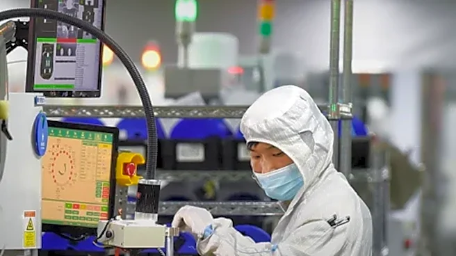
This federal investment is crucial for Arizona, a leading state in semiconductor manufacturing, as it addresses the critical need for sustainable water management within the industry. By developing advanced water reuse technologies, ASU will contribute to reducing the water footprint of chip production, which is vital for the state's water security. This initiative also supports the broader national objective of strengthening American manufacturing and ensuring a resilient domestic semiconductor supply chain. The project is expected to create good-paying jobs and foster innovation, positioning Arizona as a leader in community-beneficial technological advancements. Furthermore, the validation of these technologies at ASU's facility will provide essential data for commercial adoption, benefiting semiconductor fabs seeking to reduce water usage and improve operational resilience, while also generating new intellectual property for licensing.
What's Next?
The project will proceed in two phases: first, developing and integrating emerging treatment technologies into a mobile, pilot-scale demonstration testbed, and second, validating these technologies in manufacturing-representative conditions at ASU’s MTW facility. Quarterly stakeholder reviews will guide the progression of technologies to pilot-scale demonstration, where researchers will quantify water savings, cost reductions, and operational benefits. The ultimate goal is to bridge the gap between fundamental research and commercial deployment, making these water-saving solutions accessible to semiconductor manufacturers. This will likely lead to increased adoption of these technologies across the U.S. semiconductor industry, further enhancing water efficiency and sustainability in chip production.
Beyond the Headlines
The investment highlights a growing recognition of the interconnectedness between industrial growth, environmental sustainability, and national security. As semiconductor manufacturing expands in the U.S., particularly in water-stressed regions like Arizona, the demand for innovative water management solutions becomes paramount. This project not only addresses immediate water conservation needs but also sets a precedent for how federal funding can drive sustainable industrial practices. It underscores the role of academic institutions like ASU in translating research into practical applications that benefit both the economy and the environment. The long-term implications include a more resilient and environmentally responsible domestic semiconductor industry, potentially influencing global standards for sustainable manufacturing.