







What's Happening?
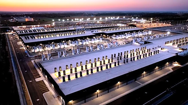
South Korean chipmaker SK Hynix has commenced construction on a new advanced packaging and research facility in West Lafayette, Indiana, representing an investment exceeding $4 billion. The facility, located at the Purdue Research Park, is slated to begin
cleanroom operations in the second half of 2028. This strategic expansion aims to meet the escalating demand for high-bandwidth memory (HBM) chips, which are crucial for AI applications. The site will house a next-generation HBM packaging line and an AI semiconductor research and development center. This investment aligns with SK Hynix's strategy to expand its AI memory operations closer to major U.S. customers such as NVIDIA, Microsoft, and Google, while also fostering research collaborations with Purdue University and developing local engineering talent. The project is expected to create approximately 7,000 direct and indirect jobs locally and enhance the resilience of the semiconductor supply chain.
Why It's Important?
This significant investment by SK Hynix in Indiana underscores the critical role of advanced packaging in the rapidly expanding AI industry. HBM chips, which stack memory vertically for faster and more power-efficient data processing, are essential for the demanding computational needs of AI. As major technology companies accelerate their efforts to build AI data centers, the demand for HBM and other advanced memory solutions has surged, leading to tighter supplies. By establishing a U.S.-based facility, SK Hynix aims to mitigate supply chain risks and strengthen its relationships with key American AI hardware developers. This move also contributes to the U.S. government's initiatives, such as the CHIPS Act, which provided $458 million in grants and up to $500 million in loans for the project, to boost domestic semiconductor manufacturing and research. The facility will enhance U.S. capabilities in advanced packaging, a crucial step in chip production, and foster innovation and job creation in the region.
What's Next?
The facility is scheduled to begin cleanroom operations in the second half of 2028. In the interim, SK Hynix will continue its construction and development efforts, likely focusing on hiring and training the necessary workforce. The company's collaboration with Purdue University is expected to deepen, fostering local talent and advancing AI semiconductor research. The success of this facility could encourage further foreign direct investment in the U.S. semiconductor sector, particularly in advanced packaging. As demand for AI continues to grow, the output from this Indiana plant will be crucial for major U.S. tech companies. The project's progress will be closely watched as a benchmark for the effectiveness of government incentives like the CHIPS Act in strengthening the domestic semiconductor supply chain and supporting the burgeoning AI industry.
Beyond the Headlines
The SK Hynix investment in Indiana highlights a broader geopolitical and economic trend: the re-shoring and diversification of critical technology supply chains. The U.S. government's backing through the CHIPS Act reflects a strategic effort to reduce reliance on overseas manufacturing for essential components like AI chips, which have significant national security implications. This move is not just about economic growth but also about technological sovereignty and resilience in the face of global supply chain disruptions and geopolitical tensions. The integration of research and development with manufacturing, as planned for the Indiana facility, signifies a holistic approach to innovation, aiming to keep the U.S. at the forefront of AI and semiconductor technology. Furthermore, the focus on HBM chips underscores the evolving architecture of computing, where memory and processing are becoming increasingly intertwined, driving new paradigms in chip design and manufacturing.