







What's Happening?
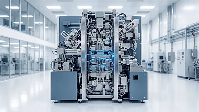
Applied Materials unveiled a multi-billion dollar research facility in Sunnyvale, California, on October 12, increasing its investment in its Equipment and Process Innovation and Commercialization (EPIC) Center to approximately $5 billion. This represents
an increase from the initially announced $4 billion in 2023. This significant boost in private investment is expanding and complexifying the U.S. semiconductor R&D sector. According to Chris Miller of Tufts University and Tristan Holtam, Applied Materials' chief strategy officer, the primary driver behind this surge in investment is the anticipated enormous profits from the current artificial intelligence (AI) frenzy. Holtam noted that the top 10 semiconductor companies' revenue has grown by about 150 percent since 2021 due to AI demand, leading to a 67 percent increase in their R&D investments.
Why It's Important?
This substantial private investment by Applied Materials is critical for accelerating semiconductor research and development in the U.S., particularly in the context of AI-driven demand. While government initiatives like the CHIPS and Science Act provide significant funding, the private sector's commitment, totaling $67 billion this year from top semiconductor companies, dwarfs federal contributions. This investment will foster innovation in material discovery, generative design of equipment, and algorithm and software development, which are essential for producing next-generation high-performance chips. The EPIC Center's model of inviting top customers like TSMC, Samsung, Micron, and Broadcom to set up operations within the lab aims to reduce the time from early-stage discoveries to chip commercialization, a process that typically takes 10 to 15 years. This collaborative approach is vital for maintaining the U.S.'s competitive edge in the global semiconductor industry.
What's Next?
The EPIC Center's operational model, which involves co-locating Applied Materials' research staff with its top customers, is expected to significantly accelerate the development and commercialization of new chip technologies. This physical proximity and collaborative environment will streamline the process of bringing prototype equipment to market, eliminating traditional points of contention and speeding up innovation cycles. While the initial partnerships are with industry leaders, the long-term goal is to reduce the time it takes for new discoveries to reach commercialization by several years. This could lead to a faster introduction of more powerful and efficient AI-ready chips, impacting various sectors from data centers to edge computing. The success of this model could also influence future R&D strategies across the semiconductor industry, potentially leading to more integrated and collaborative research environments.
Beyond the Headlines
The surge in private investment in semiconductor R&D, largely fueled by AI demand, highlights a fundamental shift in how technological innovation is being driven. It underscores the immense economic potential of AI and its cascading effects on foundational industries like semiconductors. This trend also brings to light the increasing importance of physical proximity in advanced manufacturing R&D, as the complexities of chipmaking require close collaboration between equipment manufacturers and chipmakers. Ethically, the concentration of R&D efforts among industry giants, as seen with EPIC's initial partnerships, raises questions about the accessibility of these advanced facilities for smaller companies and startups, potentially exacerbating the competitive landscape. Culturally, it signifies a renewed focus on scientific and engineering excellence within the U.S., driven by market forces and strategic national interests, potentially inspiring a new generation of innovators in these critical fields.