
What's Happening?
The global flip chip technology market is projected to grow significantly, reaching USD 37.91 billion in 2026 and expanding to USD 57.80 billion by 2032, at a Compound Annual Growth Rate (CAGR) of 7.27%.
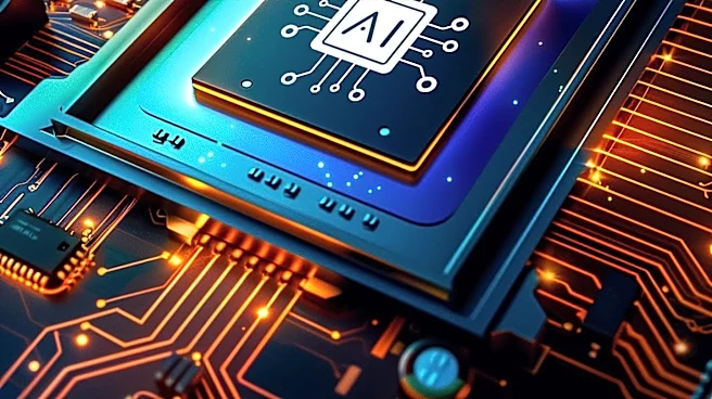
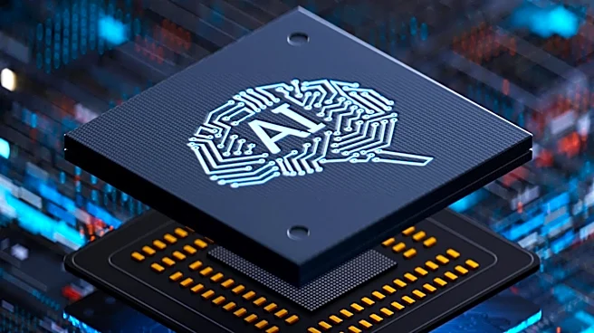
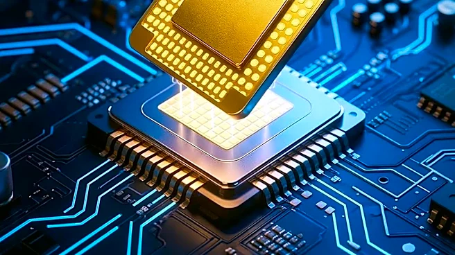
This growth is fueled by advancements in artificial intelligence (AI) processors, accelerators, memory systems, and networking components, which demand high bandwidth, dense interconnects, robust power delivery, and efficient heat removal. Flip chip technology, which connects semiconductor dies directly to substrates, offers shorter electrical paths, greater input/output density, and more compact form factors compared to traditional wire bonding. It is evolving from a standalone packaging choice into a core component of advanced packaging trends like heterogeneous integration, chiplet architectures, 2.5D and 3D packaging, and wafer-level processes.
Why It's Important?
The expansion of flip chip technology is crucial for the U.S. semiconductor industry and its ability to support next-generation computing, particularly in AI and high-performance computing. As demand for more powerful and compact electronic devices grows, the ability to integrate more functionality into smaller footprints becomes paramount. Flip chip technology directly addresses these needs by enabling higher performance and efficiency in semiconductor packaging. For U.S. companies involved in chip design, manufacturing, and advanced packaging, this trend signifies a need for continuous innovation in fine-pitch interconnects, substrate engineering, thermal management, and reliability testing. Investment in these areas will be critical for maintaining competitiveness and ensuring the U.S. remains at the forefront of technological advancement in AI and other high-tech sectors.
What's Next?
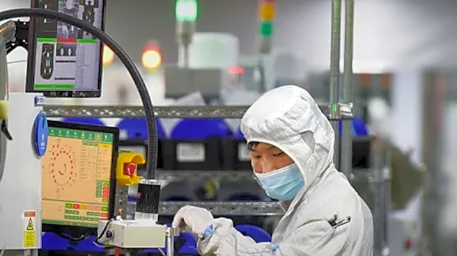
The flip chip technology market will continue to see advancements in packaging capabilities, substrate materials, and manufacturing precision. The increasing demand for AI-driven applications will push for further innovations in high-density systems, requiring enhanced thermal cycling and electromigration resistance. AI-assisted design and manufacturing processes are expected to improve defect detection, process optimization, predictive maintenance, and yield analysis, further accelerating the adoption and efficiency of flip chip technology. Decision-makers in the semiconductor industry will need to strategically assess opportunities while carefully managing integration, manufacturing, and supply-chain risks to capitalize on this growth. The focus will remain on developing solutions that offer superior performance in smaller, more power-efficient packages.
Beyond the Headlines
The evolution of flip chip technology into a core component of heterogeneous integration and 3D packaging signifies a fundamental shift in how semiconductors are designed and manufactured. This move towards more complex, integrated architectures has profound implications for the entire electronics industry, enabling the creation of devices with unprecedented capabilities. It also highlights the increasing importance of packaging as a key differentiator, moving beyond simply protecting the chip to actively enhancing its performance. This trend could lead to new intellectual property developments in packaging science and materials engineering, fostering interdisciplinary collaboration. Furthermore, the reliance on precise manufacturing and advanced materials introduces new challenges in supply chain management and quality control, emphasizing the need for robust, traceable manufacturing processes to ensure reliability and performance in critical applications.