



What's Happening?
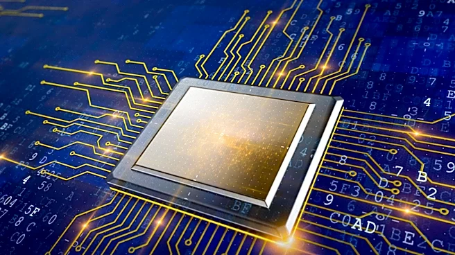
TSMC is redefining its approach to semiconductor scaling by moving beyond traditional transistor density. The company is focusing on system-level integration, utilizing advanced packaging technologies like CoWoS and SoIC, and incorporating photonics.
This shift addresses the bottleneck in data transmission rather than computational power, emphasizing the importance of memory bandwidth and die-to-die interconnects. TSMC's 3DFabric platform exemplifies this strategy, combining cutting-edge processes with advanced packaging to enhance system performance.
Why It's Important?
TSMC's strategic shift reflects a broader industry trend towards system-level optimization in semiconductor manufacturing. As AI and high-performance computing demand more efficient data processing, the integration of multiple dies and advanced packaging becomes crucial. This approach not only improves energy efficiency but also supports the development of more powerful and compact computing systems. TSMC's innovations could set new standards in the semiconductor industry, influencing future technology development and manufacturing practices.
What's Next?
TSMC will continue to develop its 3DFabric platform, with plans to enhance its CoWoS and SoIC technologies. The company aims to further integrate optical interconnects, potentially revolutionizing data transmission in semiconductor systems. As TSMC advances its technology, it may face challenges related to manufacturing complexity and cost. However, successful implementation could solidify TSMC's position as a leader in semiconductor innovation, driving further advancements in AI and high-performance computing.