




What's Happening?
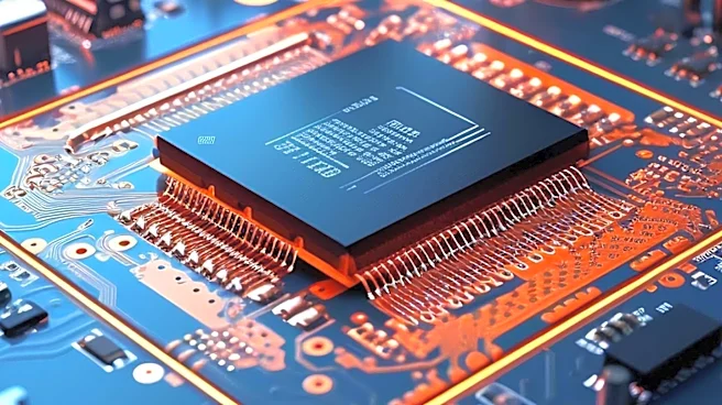
Atomica has introduced its AI Photonic Integration Platform, a microfabrication solution designed to overcome challenges in integrating photonics with other critical components in AI infrastructure hardware. This platform aims to enable the scalable manufacturing
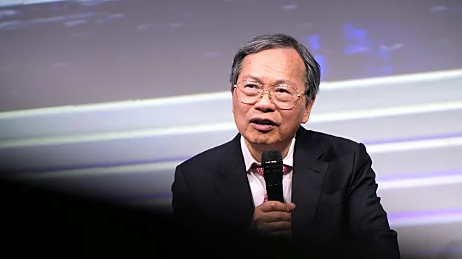
of complex AI systems by bringing together diverse elements such as electronics, memory, and thermal management structures. The platform utilizes a configurable microfabrication pathway that includes interposers, vias, bonding, optical alignment, and wafer-level packaging. It supports various process layers like silicon and glass interposers, through-silicon vias, redistribution layers, and customer-specific process layers. The core problem it addresses is the difficulty of combining components built on different substrates and materials, each with unique alignment, stress, thermal, and reliability requirements, without compromising performance or manufacturability. According to Eldon Klaassen, CEO of Atomica, future advancements in AI hardware will stem from this kind of comprehensive integration rather than single chip improvements.
Why It's Important?
This development is crucial for the advancement of AI hardware, particularly in data centers, where packaging and interconnectivity are becoming significant limiting factors. The increasing demand for AI accelerators, high-bandwidth memory integration, chiplet packages, and co-packaged optics necessitates solutions that can handle complex integration challenges. Current system constraints often arise from issues like bandwidth, interconnect density, signal integrity, thermal management, and precise optical alignment, even before processors reach their theoretical limits. Atomica's platform offers a pathway to integrate these disparate elements with the precision and repeatability required for mass production, which is essential for the continued growth and efficiency of AI infrastructure. By streamlining the integration process, the platform can help accelerate the deployment of more powerful and energy-efficient AI systems, impacting industries reliant on advanced computing capabilities.
What's Next?
Atomica's AI Photonic Integration Platform is positioned as the third in its series of AI infrastructure platforms, following its AI Optical Connectivity Platform and AI Optical Source Platform. The company intends for these platforms to cover complementary aspects of the AI optical hardware stack, with the new integration platform specifically focusing on tying optical functions into broader substrate and packaging structures. Target applications for this platform include AI accelerators, high-bandwidth memory integration, chiplet packages, data-center switches, optical I/O modules, co-packaged and near-packaged optics, photonic integrated circuit packaging, optical engines, and external laser-source packages. The success of this platform will likely lead to more efficient and powerful AI hardware, potentially reducing the cost and increasing the accessibility of advanced AI technologies across various sectors. Further adoption by manufacturers will depend on the platform's demonstrated ability to deliver on its promises of scalability and performance.
Beyond the Headlines
The introduction of Atomica's AI Photonic Integration Platform highlights a fundamental shift in the approach to AI hardware development. The focus is moving beyond individual component performance to the intricate challenges of system-level integration. This signifies a recognition that the physical limitations of packaging and interconnects are now as critical as the computational power of the chips themselves. The platform's emphasis on manufacturability at scale suggests a long-term vision for industrializing advanced AI hardware, moving it from specialized labs to widespread commercial deployment. This could have profound implications for the energy consumption of data centers, the speed of AI model training, and the overall economic viability of AI-driven solutions. The ability to precisely integrate optical, electronic, memory, and thermal structures could also foster new innovations in chip design and system architecture, potentially leading to entirely new categories of AI hardware.