







What's Happening?
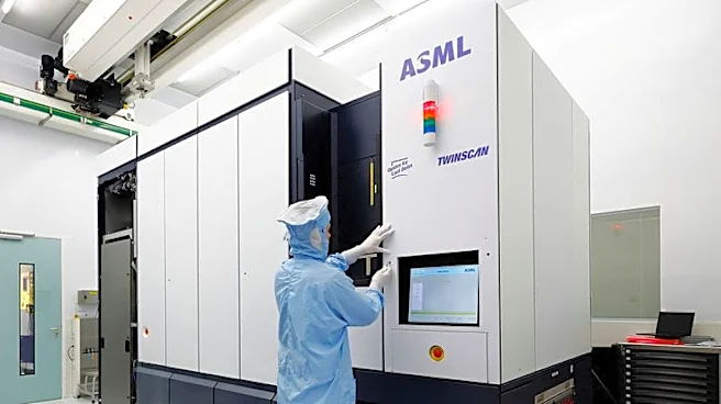
ASML has announced that Intel Foundry is now utilizing its High Numerical Aperture (High NA) Extreme Ultraviolet (EUV) technology in high-volume production on the Intel 18A process node. This marks the first instance of High NA EUV machines being used
for large-scale silicon production. Intel initially installed ASML's first-generation EXE:5000 High-NA EUV machine in 2024 for research purposes, followed by the TWINSCAN EXE:5200B model in December 2025. The newer model enhances productivity through a higher-power EUV light source, improved wafer stocker architecture, and tighter alignment controls. High NA EUV technology improves upon existing EUV lithography by enhancing optics, control, and tooling, rather than using shorter-wavelength light. Intel's 18A node is 'dual qualified' on High NA EUV, meaning it is validated using both High NA and standard EUV lithography machines, allowing Intel to match silicon yields across both platforms.
Why It's Important?
The adoption of High NA EUV technology by Intel represents a significant advancement in semiconductor manufacturing, enabling the production of denser and more efficient transistors. This technological leap is expected to drive the performance of next-generation CPUs, GPUs, and other chips to new heights. Intel's early adoption of this technology could provide a competitive edge over other manufacturers like TSMC, which plans to continue using Low-NA EUV machines until 2029. The successful implementation of High NA EUV could lead to broader adoption within Intel and potentially influence the semiconductor industry's future technological direction.
What's Next?
Intel's use of High NA EUV technology is likely to expand, with future process nodes, such as the anticipated A14 node, potentially relying exclusively on this advanced lithography. The data and insights gained from the current production will help refine the system setup, paving the way for broader utilization. As Intel continues to integrate High NA EUV into its manufacturing processes, other semiconductor companies may reassess their strategies regarding the adoption of this technology, potentially accelerating its industry-wide implementation.