
What's Happening?
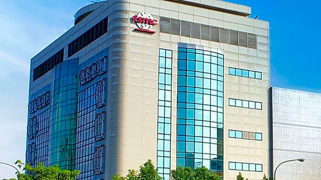
TSMC and ASML have announced a collaborative industry initiative aimed at transitioning to 12-inch photomasks to maximize the value of High NA Extreme Ultraviolet (EUV) lithography. This initiative, revealed
on September 7 in advance of the SPIE Bacus Conference, seeks to establish a 12-inch mask pilot line by 2031, with full lithography system readiness for advanced node production anticipated by 2033. While High NA EUV technology will initially be adopted using current 6-inch masks, the shift to larger 12-inch masks is expected to significantly enhance fab productivity, reduce chipmaking costs, and eliminate stitching constraints. This transition is crucial for advanced chip manufacturers to fully leverage High NA EUV, making future generations of leading-edge chips more cost-effective. Christophe Fouquet, president & CEO of ASML, stated that the adoption of High NA EUV will progressively increase along the device scaling roadmap, supported by 12-inch masks to meet the demand for smaller, faster, and more energy-efficient chips. TSMC intends to implement ASML’s High NA technology in high-volume manufacturing for advanced nodes starting in 2030, anticipating an increase in the number of layers requiring High NA EUV due to complex transistor architectures for AI applications.
Why It's Important?
This collaboration between TSMC and ASML is critically important for the U.S. semiconductor industry and the broader technology sector. The transition to 12-inch photomasks for High NA EUV lithography represents a significant leap in semiconductor manufacturing capabilities, enabling the production of more advanced, powerful, and energy-efficient chips. This directly impacts industries reliant on cutting-edge semiconductors, such as artificial intelligence, high-performance computing, and consumer electronics. By lowering chipmaking costs and increasing productivity, this initiative can help maintain the U.S.'s competitive edge in semiconductor innovation and reduce reliance on foreign manufacturing for critical components. The development of more sophisticated chips is essential for driving advancements in AI applications, which require increasingly complex transistor architectures. Companies like TSMC, a major supplier to U.S. tech giants, will be able to produce these advanced components more efficiently, potentially leading to faster innovation cycles and more affordable high-tech products for consumers and businesses. The initiative also underscores the importance of industry-wide collaboration to overcome complex technological challenges, benefiting the entire semiconductor value chain.
What's Next?
The immediate next steps involve establishing a 12-inch mask pilot line by 2031, followed by achieving full lithography system readiness for advanced node production by 2033. This timeline indicates a long-term commitment to evolving semiconductor manufacturing processes. The initiative will require continued collaboration among semiconductor manufacturers, mask suppliers, and other partners to ensure a smooth transition and widespread adoption of the new technology. TSMC's plan to use ASML’s High NA technology in high-volume manufacturing for advanced nodes starting in 2030 suggests that the industry is preparing for a significant shift in production methods. As technology nodes advance, the demand for High NA EUV will grow, particularly for AI applications, necessitating continuous innovation in lithography. The success of this initiative will likely influence future investments in semiconductor research and development, potentially leading to further advancements in chip design and manufacturing processes. Stakeholders across the tech industry will be closely watching the progress of this collaboration, as it will directly impact their ability to develop next-generation products.
Beyond the Headlines
Beyond the immediate technical and economic benefits, this initiative highlights a deeper trend in the semiconductor industry: the increasing complexity and cost of advanced chip manufacturing. The need for collaborative efforts between industry giants like TSMC and ASML to develop new lithography techniques underscores the immense challenges involved in pushing the boundaries of Moore's Law. This also raises questions about the accessibility of cutting-edge chip technology, as the high initial investment and specialized expertise required could further consolidate power among a few dominant players. The focus on AI applications as a primary driver for these advancements suggests a future where AI capabilities are deeply intertwined with hardware innovation, potentially leading to a virtuous cycle of demand for more powerful chips and more sophisticated AI. Furthermore, the environmental impact of such advanced manufacturing processes, particularly in terms of energy consumption and resource use, will become an increasingly important consideration as the industry scales up production of these highly complex components.