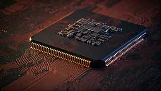


Pioneering Advanced Packaging
India has embarked on a crucial mission to establish a comprehensive semiconductor ecosystem, with the India Semiconductor Mission (ISM) at its core. Launched
in 2021 with a substantial investment of Rs 76,000 crore, this state-backed initiative aims to cover every aspect of chip manufacturing, from design and fabrication to assembly and testing. A pivotal development within this ambitious scheme is the foundation stone laid for India's first advanced 3D chip packaging unit in Bhubaneswar, Odisha. This facility is not just another manufacturing plant; it represents a strategic leap towards mastering cutting-edge technology. The government views this project with great importance, recognizing its potential to put India on the global map for advanced chip packaging. This groundbreaking facility is expected to produce specialized glass substrate panels and advanced 3D heterogeneous integration (3DHI) modules, catering to high-demand sectors like artificial intelligence, 5G telecommunications, national defence, and robust data centers. The project has already attracted significant backing from industry giants, including Intel and Lockheed Martin, alongside investments from venture capital and private equity firms, underscoring its strategic value and commercial viability.
The 3D Glass Advantage
The newly established facility in Odisha is set to revolutionize chip manufacturing by moving beyond traditional silicon wafers and 2D planar packaging. Instead, it will leverage unique glass-based substrates and sophisticated 3D stacking techniques. This innovative approach allows for the vertical integration of multiple chip components, a method that dramatically enhances computing power while maintaining a compact physical footprint. The advantages of employing glass substrates are manifold: they offer superior thermal stability, crucial for high-performance computing, and exhibit reduced signal loss, leading to more efficient data transmission. Furthermore, glass substrates enable a higher degree of precision, which is essential for manufacturing at advanced technology nodes. This shift towards 3D glass chip technology is directly aligned with the evolving demands of modern computing. As devices like smartphones, autonomous vehicles, and complex AI systems require increasingly more processing power within shrinking dimensions, the ability to stack chips vertically and integrate diverse components such as logic units, memory modules, and sensors becomes indispensable. This concept, known as heterogeneous integration, is the key to unlocking faster AI algorithms, building more energy-efficient data centers, and developing sophisticated defence electronics.
Navigating Moore's Law
The groundbreaking advancements in 3D glass chip technology are also a response to the evolving landscape of Moore's Law. Originally posited in 1965 by Gordon Moore, co-founder of Intel, this influential principle predicted a doubling of transistors on a chip roughly every two years, a trend that fueled decades of exponential growth in computing power and cost reduction. However, as semiconductor manufacturing approaches fundamental physical and thermal limitations at the most advanced nodes, the pace of this progress has naturally slowed. The industry is now actively seeking alternatives to sustain performance improvements, and advanced packaging techniques like chiplets and 3D integration are at the forefront of this quest. The Odisha facility's focus on 3D packaging using glass substrates is a direct effort to circumvent these limitations and continue the trajectory of performance enhancement. This innovative approach aims to achieve greater processing density and efficiency, thereby extending the spirit of Moore's Law through novel architectural and material solutions, positioning India at the cutting edge of this technological evolution.
Project Scale and Impact
The facility in Odisha represents a significant investment and a substantial leap in manufacturing capacity. It is slated to produce an impressive 70,000 glass panels annually, alongside 50 million assembled units. Furthermore, the project is expected to yield approximately 13,000 advanced 3DHI modules, highlighting its contribution to specialized semiconductor components. This state-of-the-art plant is one of two approved projects within Odisha under the India Semiconductor Mission, underscoring the state's growing importance in the national semiconductor strategy. Beyond its technological significance, the project is poised to create a considerable economic impact, generating an estimated 2,500 direct and indirect employment opportunities. This job creation is vital for the region, contributing to economic growth and skill development. The project's success is being closely monitored by the government, given its pioneering nature and potential to reshape India's position in the global semiconductor supply chain, offering a glimpse into the future of advanced chip manufacturing.
India's Semiconductor Ambitions
The India Semiconductor Mission, established in 2021 with a massive Rs 76,000-crore budget, is a comprehensive, government-backed strategy to cultivate a complete indigenous semiconductor ecosystem. This mission encompasses the entire value chain, from the intricate design processes to the large-scale manufacturing of fabrication plants, and extends to display fabrication. To date, the ISM has greenlit ten semiconductor projects spread across six different states, attracting an aggregate investment exceeding Rs 1.6 lakh crore. These approved projects include critical fabrication facilities, essential OSAT (Outsourced Semiconductor Assembly and Test) units, and initiatives offering design-linked incentives to foster innovation. Looking ahead, the government is reportedly preparing the next phase of this strategic plan, potentially involving an outlay of around $11 billion. While the first iteration of the ISM focused primarily on attracting established chipmaking infrastructure to India, the upcoming phase, ISM 2.0, is anticipated to broaden its scope. It is expected to provide enhanced support for ancillary industries, such as specialized gases, chemicals, and capital goods, which are crucial for a robust semiconductor ecosystem. Moreover, ISM 2.0 may feature a more pronounced emphasis on the design segment, with incentives potentially being tied to the amount of market capital companies successfully raise, signaling a maturing and evolving national semiconductor strategy.