
The Simple Logic on Paper
At its heart, a logic gate is a tiny decision-maker. It takes one or more inputs in the form of electrical signals (either 'on' for a 1 or 'off' for a 0) and produces a single output signal based on a specific
rule. The most basic gates are AND, OR, and NOT. An AND gate only outputs a '1' if all its inputs are '1'. An OR gate outputs a '1' if at least one of its inputs is '1'. And a NOT gate simply inverts the input, turning a '1' into a '0' and vice-versa. Using these simple rules, you can combine gates to perform any mathematical or logical operation imaginable, from adding two numbers to running a complex algorithm. They are the fundamental building blocks of all digital circuits.
From Idea to Microscopic Switch
Here's the first layer of complexity: a logic gate isn't a single, discrete object. It's a concept made real by arranging microscopic switches called transistors. Today, these are almost exclusively a type called MOSFETs. Think of a transistor as a microscopic, electrically controlled switch with no moving parts. By connecting a few of these transistors in a specific pattern, you create the behavior of an AND, OR, or NOT gate. For example, wiring two transistors in a series can create an AND gate; current flows to produce a '1' output only if both switches are on. This leap from a logical rule to a physical arrangement of components is where the elegant simplicity starts to get messy.
The Tyranny of Extreme Miniaturization
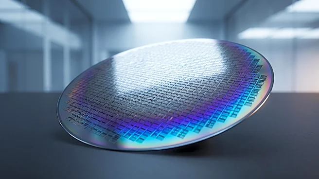
The real complexity comes from scale. A modern processor doesn't have a few dozen transistors; it has tens of billions packed onto a silicon chip the size of a thumbnail. This is the result of Moore's Law, the observation that the number of transistors on a chip doubles roughly every two years. But shrinking transistors isn't just a matter of making everything smaller. The manufacturing process, known as fabrication, is one of the most precise and difficult engineering feats ever achieved. It takes place in hyper-clean rooms where even a single speck of dust can ruin a chip. The process involves depositing and etching away layers of materials with atomic-level precision. Even minor defects can render a chip useless, making yield optimization a constant battle.
When the Laws of Physics Fight Back
At the scale of modern transistors—just a few nanometers wide—the familiar rules of classical physics begin to break down, and the bizarre world of quantum mechanics takes over. One of the biggest problems is called quantum tunneling. The insulating barriers designed to stop electrons from flowing when a transistor is 'off' become so thin that electrons can essentially 'teleport' right through them. This creates leakage currents that waste power and generate excess heat. Speaking of heat, as transistor density increases, so does the heat they produce. For years, a principle called Dennard scaling meant that as transistors got smaller, their power density stayed constant. But that rule broke down around 2005. Now, we can add more transistors, but we can't always run them at full speed without the chip overheating. This is why clock speeds for processors haven't dramatically increased in over a decade.
The Billion-Dollar Problem
Finally, there is the sheer economic complexity. Building a new semiconductor fabrication plant, or 'fab,' can cost over $20 billion. These facilities are incredibly sophisticated, requiring a global supply chain for rare materials, specialized chemicals, and unbelievably precise machinery. Disruptions in this supply chain, geopolitical tensions, and a shortage of skilled workers all add layers of difficulty and risk. The cost of research and development to overcome challenges like quantum tunneling and heat dissipation is immense. The simple logic gate on a whiteboard is free; the billions of them in your phone represent one of the most expensive and complex manufacturing ecosystems on Earth.