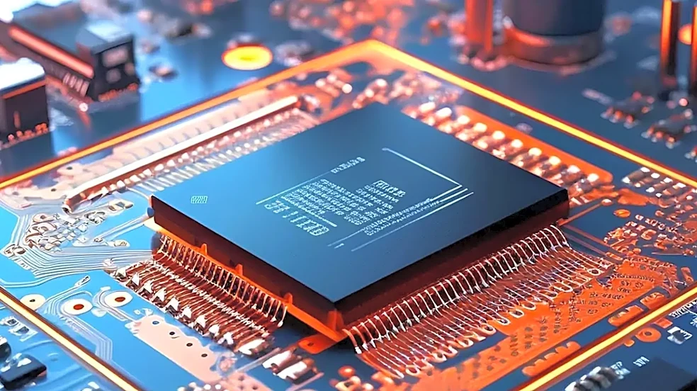









On the surface, an Application-Specific Integrated Circuit (ASIC) seems refreshingly straightforward. It’s a microchip designed to do one thing, and one thing only. But this single-mindedness is deceptive. Here’s the real story.
The Seductive Simplicity of a Specialist
An ASIC is the ultimate
specialist. Unlike a general-purpose CPU in your laptop—a jack-of-all-trades that can run a web browser, a spreadsheet, or a game—an ASIC is purpose-built. Think of a CPU as an adjustable wrench, useful for many different nuts and bolts but not perfect for any single one. An ASIC is like a custom-molded socket wrench built for one specific bolt, and it turns that bolt with incredible speed and efficiency. This is why they are essential in devices from network switches to Bitcoin miners and smartphones, where performance and power efficiency are critical. Because they only have one job, it’s easy to assume they are simple to create. Just design the circuit for that one task, and you're done. Right?
The Multi-Million Dollar Blueprint
The journey from an idea to a finished ASIC is a marathon of high-stakes engineering that can take years. It begins with teams of highly specialized engineers who use complex software to design the chip's functionality, writing hundreds of thousands or even millions of lines of code in a hardware description language. This digital blueprint must be perfect. Unlike a software update you can push to fix a bug, an error in an ASIC’s hardware design is permanent. A single flaw means the entire project can fail, turning a massive investment into a worthless piece of silicon. This initial design phase alone represents an enormous upfront cost known as Non-Recurring Engineering, or NRE, which can range from hundreds of thousands to tens or even hundreds of millions of dollars before a single physical chip is ever made.
The Terrifying World of Verification
If designing the chip is hard, making sure it works is even harder. The verification process, where engineers test the digital design against every conceivable scenario, often consumes over half of the entire project timeline. It's an exhaustive and paranoid search for bugs that could cripple the chip. Teams build complex virtual test environments and run billions of simulations to hunt for flaws in logic, timing, or power consumption. This isn't just about making sure the chip does what it's supposed to do; it's about proving it will never do what it's not supposed to do, under any circumstances. Missing a single corner-case bug before manufacturing can lead to a 're-spin'—a do-over that costs millions of dollars and months of delays.
There Are No Small Mistakes in Manufacturing
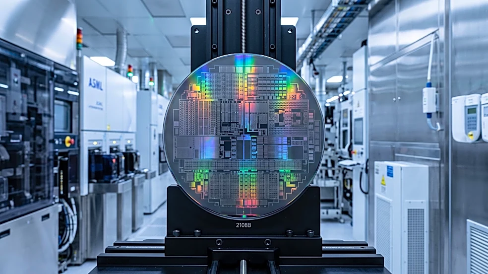
Once the design is verified and declared 'frozen', it’s sent to a semiconductor foundry for manufacturing—a process called 'tape-out'. This is the point of no return. The foundry uses the design to create a set of 'masks', which are like incredibly precise stencils used in a process called photolithography to etch the circuit onto silicon wafers. The mask set for a modern chip can cost millions of dollars on its own. The manufacturing process itself is a marvel of cleanroom robotics and atomic-scale precision. After the wafers are fabricated, they are tested, cut into individual chips (or 'dies'), and packaged. Any error in this entire chain, from design to packaging, can render the final product useless. The high NRE costs and complexity mean ASICs are only viable for products that will be produced in very high volumes, allowing the initial investment to be spread out.