


It's a Skyscraper, Not a Suburb
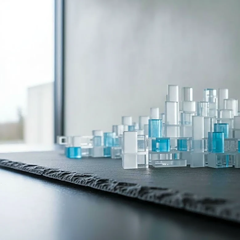
The first surprise with HBM is its physical form. Traditional graphics memory, known as GDDR, consists of individual chips spread out on the graphics card's circuit board, like houses in a suburb. HBM, on the other hand, is a silicon skyscraper. It stacks
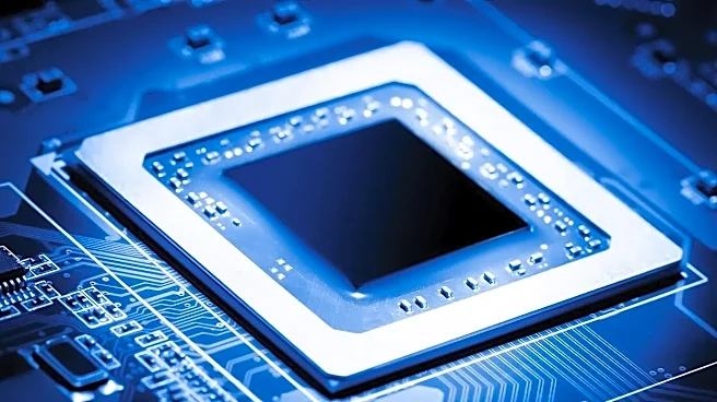
DRAM memory chips vertically on top of each other and connects them with microscopic vertical channels called Through-Silicon Vias (TSVs). This entire memory stack is then placed directly on the same package as the GPU processor itself, connected by a high-speed silicon pathway called an interposer. This design is radically different. Instead of data traveling across a circuit board, it zips between the processor and memory in millimeters. This proximity is key to its performance, but it also means the memory is an integral part of the GPU package, not a separate component you can swap out.
The Speed Isn't What You Think
When we think of speed, we often think of clock speed, measured in megahertz (MHz). Herein lies the second surprise: HBM often runs at a lower clock speed than its GDDR counterparts. This can be confusing. How can it be faster if the number is lower? The answer is bandwidth. Think of it like a highway. GDDR is a fast sports car on a narrow road, while HBM is a fleet of buses on a massive, multi-lane superhighway. HBM achieves its incredible performance not through raw clock speed but through an incredibly wide data bus. A typical HBM stack has a 1024-bit interface, while GDDR6 uses a much narrower 32-bit bus per channel. This means HBM can move vastly more data at once, even if it's moving it at a lower clock rate. This firehose of data is exactly what power-hungry AI and high-performance computing tasks need to keep the processor cores fed.
The Price Is Part of the Feature
The third and often most jarring surprise for new users is the cost. HBM is exceptionally expensive, and its price has a profound impact on the final cost of a GPU. As of 2026, HBM memory can account for 30-40% of the total manufacturing cost of a high-end AI accelerator. This isn't just the price of the memory chips themselves; the intricate process of stacking the dies, creating the silicon interposer, and packaging it all together with the GPU is complex and costly. For some of the latest AI GPUs, the cost of the HBM3e memory alone can be several times higher than the cost of the main processor die it serves. This high cost is a primary reason why HBM is reserved for top-tier professional cards, data center GPUs, and a handful of flagship consumer products where performance at any cost is the main goal.
You Often Get Less of It
Given the high cost and complex architecture, the fourth surprise is that GPUs with HBM sometimes have less total memory capacity than high-end consumer cards using GDDR. For example, you might see a gaming card with 24GB of GDDR6, while a professional HBM-equipped card might have a similar or even slightly lower capacity. This seems counterintuitive for a premium technology. However, this is another engineering trade-off. For the workloads HBM is designed for—like training massive AI models—the bottleneck isn't always the total amount of VRAM, but the speed at which data can be moved in and out of it. The priority is eliminating the 'memory wall' by providing unparalleled bandwidth, ensuring the powerful processing cores are never left waiting for data. The capacity is still substantial and growing with each generation, but the focus remains firmly on bandwidth over sheer gigabytes.