






The Golden Age: A Free Lunch from Physics
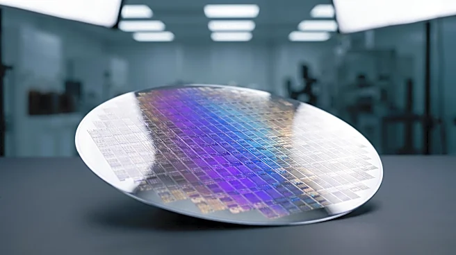
First, let's talk about what Dennard scaling was. Back in 1974, an IBM engineer named Robert H. Dennard co-authored a paper that laid out a beautiful principle for making transistors—the tiny on-off switches that are the building blocks of modern computing.
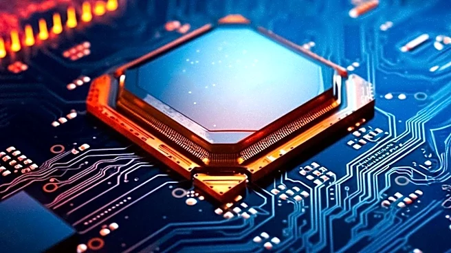
The rule, which became known as Dennard scaling, stated that as you made transistors smaller, their power density remained constant. In simple terms, this meant you could shrink a transistor, make it faster, and it wouldn't get hotter per unit of area. This was a gift from physics. It allowed chip manufacturers to not only cram more transistors onto a chip every couple of years, following Moore's Law, but also to crank up the clock speeds without the chip melting. The combination of these two laws gave us decades of exponential growth, taking us from room-sized computers to the supercomputers we carry in our pockets.
Hitting the Power Wall
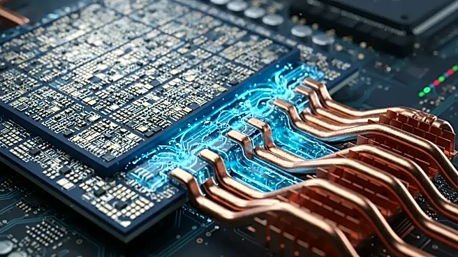
Around 2005, the free lunch ended. As engineers pushed to make transistors ever smaller, they slammed into a fundamental physical barrier often called the "power wall." At incredibly small sizes, transistors started to misbehave. The primary culprit was leakage current. Even when a transistor was supposed to be "off," electrons would still leak through. This leakage generated waste heat. While engineers could still shrink transistors, they could no longer proportionally lower the voltage needed to operate them. Continuing to shrink them and pack them closer together meant power density began to skyrocket, turning cutting-edge chips into tiny, inefficient hotplates. The clock speed race, which had seen processors jump from megahertz to gigahertz, abruptly stalled. The magic formula that had driven the industry for 30 years was broken.
The Great Disagreement: Architects vs. Physicists
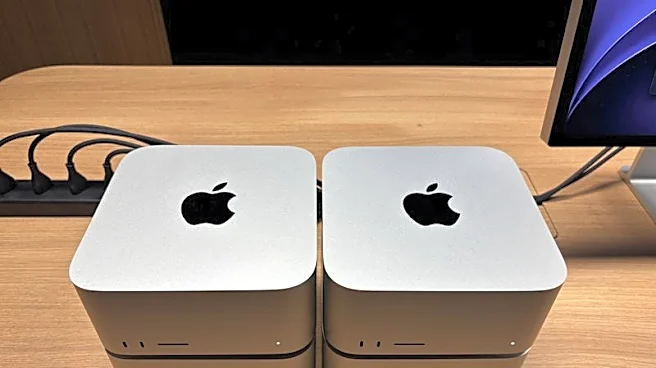
This is where the disagreement among senior engineers really begins. It’s not about whether Dennard scaling ended—everyone agrees it did. The debate is about what to do next, and it has split the field into two main camps. On one side are the Architects. This group believes the battle for efficiency at the individual transistor level is largely over. For them, the path forward is through clever design and specialization. Instead of making one core that does everything super-fast, they design chips with multiple, specialized cores. This is the philosophy behind Apple's M-series chips, which have different cores for high-performance and high-efficiency tasks, plus dedicated engines for graphics and AI. The architects work around the physics problem with smarter blueprints. On the other side are the Material Scientists and Physicists. This group isn't ready to give up on the transistor itself. They argue that while the simple scaling of silicon is over, new materials and new structures can still deliver gains. They are exploring exotic materials beyond silicon, 3D stacking techniques to build chips vertically, and new transistor designs like Gate-All-Around (GAA) to better control leakage. Their goal is to revive the spirit, if not the letter, of Dennard scaling by fundamentally changing what transistors are made of and how they are built.
How This Debate Shapes Your Devices Today
This engineering conflict isn't just academic; it directly shapes the technology you use every day. The Architects' focus on specialized hardware is why your smartphone can perform complex AI tasks like real-time language translation without draining its battery in minutes. It’s why Nvidia's GPUs are essential for the machine learning revolution. These are wins for specialized architecture. Meanwhile, the steady, incremental improvements in battery life and performance in the latest flagship devices are often thanks to the Physicists' work, introducing new materials and manufacturing processes that eke out a little more efficiency each generation. The entire industry is now in a period of what some call "Divergent Scaling," where progress comes from many different directions at once instead of a single, predictable path.