


What's Happening?
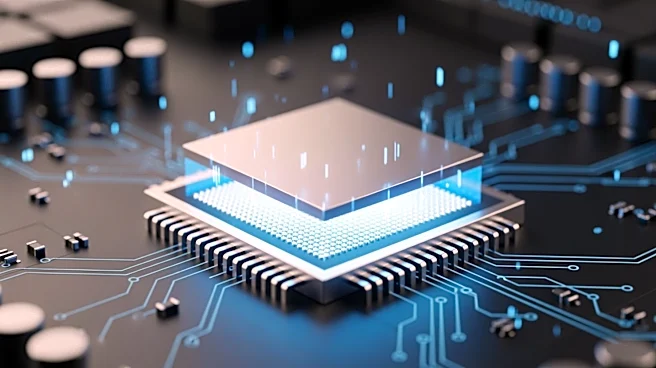
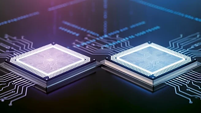
Bruker Corporation has announced the accelerated development of its photothermal AFM-IR spectroscopy capabilities to address challenges in semiconductor research. As device architectures shrink and systems become more complex, Bruker is expanding the use
of AFM-IR beyond contamination analysis into areas like EUV photoresist patterning and advanced materials for transistor scaling. In collaboration with imec, a leading research hub, Bruker has installed its Dimension IconIR system to evaluate nanoscale chemical characterization's impact on semiconductor process development. This partnership aims to enhance understanding of material behavior and interfaces critical to next-generation semiconductor technologies.
Why It's Important?
Bruker's investment in photothermal AFM-IR technology is significant for the semiconductor industry, which faces increasing demands for precision and complexity in device manufacturing. The ability to conduct nanoscale chemical analysis provides insights that are crucial for developing advanced semiconductor materials and processes. This technology supports the industry's push towards smaller, more efficient devices, which are essential for applications in AI and high-performance computing. The collaboration with imec underscores the importance of research partnerships in driving innovation and addressing emerging challenges in semiconductor metrology.