What's Happening?
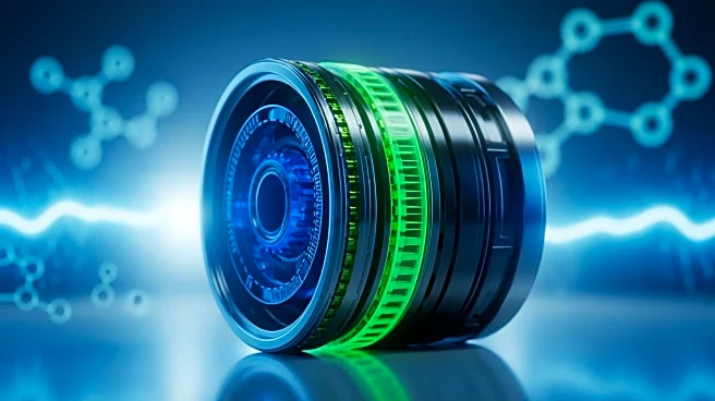
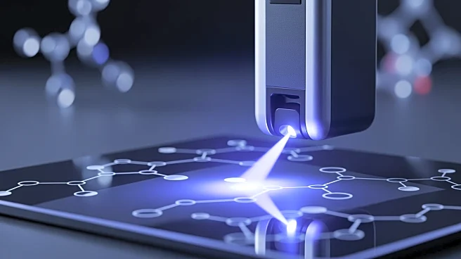
Recent advancements in optical spectrometry have led to the development of a compact ultraviolet (UV) spectral imager, which addresses the limitations of traditional benchtop systems. These systems, while
crucial for scientific research and industrial applications, are often too bulky for on-chip integration or in situ spectral analysis. The new spectral imager expands the operational range of miniaturized spectrometers into the UV and deep-UV range, which are essential for physical, chemical, biological, and pharmaceutical analysis. The device features a vertically integrated n–p–n cascaded photodiode architecture that allows for ultrafast nanosecond-scale response, enabling high-speed, real-time spectral capture. This innovation supports both single-pixel and high-resolution imaging without the need for external optics, facilitating large-scale, high-resolution spectral imaging. Additionally, the platform is compatible with mature semiconductor fabrication processes, allowing for wafer-scale production and scalable integration into dense photodiode arrays.
Why It's Important?
The development of this compact UV spectral imager is significant for several reasons. It overcomes the size and complexity challenges of conventional systems, making it possible to integrate spectral analysis capabilities into smaller, more versatile devices. This advancement is particularly important for the pharmaceutical industry, where precise and rapid analysis of materials is crucial. The ability to perform high-speed, real-time spectral capture can enhance the efficiency and accuracy of pharmaceutical development and quality control processes. Furthermore, the compatibility with existing semiconductor fabrication processes means that this technology can be produced at scale, potentially reducing costs and increasing accessibility for various applications in scientific research and industrial settings.
What's Next?
The next steps for this technology involve moving from lab prototypes to deployable systems. The compatibility with semiconductor fabrication processes suggests that large-scale production is feasible, which could lead to widespread adoption in industries that require precise spectral analysis. As the technology matures, it may also be adapted to cover visible wavelengths by tuning the alloy composition in the active region of the photodiode. This could further expand its applications across different fields, including environmental monitoring and medical diagnostics. Stakeholders in the pharmaceutical and scientific research sectors are likely to monitor these developments closely, as the technology promises to enhance analytical capabilities significantly.