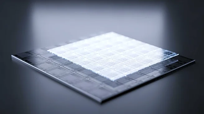


What's Happening?
Forge Nano has announced a breakthrough in semiconductor manufacturing with its high-speed atomic layer deposition (ALD) coatings, achieving a 1000:1 aspect ratio. This innovation addresses a major bottleneck in semiconductor production, enabling faster and more efficient manufacturing of next-generation AI chips and 3D architectures. The company's patented turbulent flow technology allows for defect-free coatings at production scale, significantly improving yield and reducing costs.
Why It's Important?
This development could transform the semiconductor industry by enhancing the production capabilities of AI chips and 3D-stacked devices, which are critical for advanced computing applications. By overcoming the limitations of traditional ALD processes, Forge Nano's
technology could lead to more efficient and cost-effective semiconductor manufacturing. This has implications for the competitiveness of U.S. semiconductor companies, potentially strengthening their position in the global market and supporting national security interests by advancing domestic chip production capabilities.
What's Next?
Forge Nano's technology is expected to be adopted by semiconductor manufacturers seeking to improve their production processes. The company may pursue further partnerships and collaborations to expand its market presence. The semiconductor industry will likely see increased competition as companies strive to integrate this new technology into their manufacturing processes, potentially leading to faster innovation cycles and new product developments.