


What's Happening?
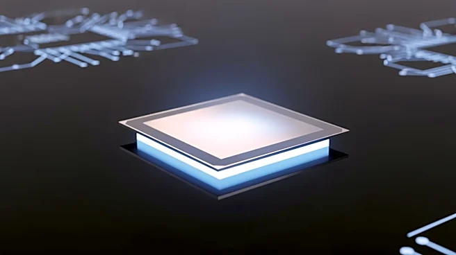
Researchers have developed a ZnS:Mn/ZnO heterostructure array chip that significantly boosts mechanoluminescence through type II electron transition. The chip is constructed using a co-sputtering technique and features a porous surface morphology. The heterostructure enhances
light absorption and emission, providing high resolution for stress detection. The chip's design allows for adjustable pixel sizes, making it suitable for various applications. The study highlights the potential for integrating mechanoluminescence into stress sensors and electronic skin, offering new possibilities for high-precision force recognition.
Why It's Important?
This advancement in mechanoluminescence technology could lead to the development of next-generation stress sensors and electronic skin, with applications in robotics and ethology research. The ability to detect small stress levels with high resolution is crucial for creating more sensitive and accurate sensors. The research also demonstrates the potential for integrating mechanoluminescence into semiconductor processes, paving the way for widespread adoption in various industries. The findings could influence the design of future electronic devices, enhancing their functionality and performance.
What's Next?
The researchers plan to explore further applications of the ZnS:Mn/ZnO heterostructure in integrated array systems. The technology could be used to develop chips for real-time stress detection and trajectory recording. The study may lead to collaborations with industry partners to commercialize the technology and expand its use in practical applications. Continued research could focus on optimizing the heterostructure design and exploring new materials to enhance mechanoluminescence performance.