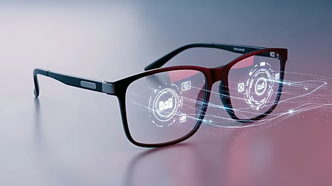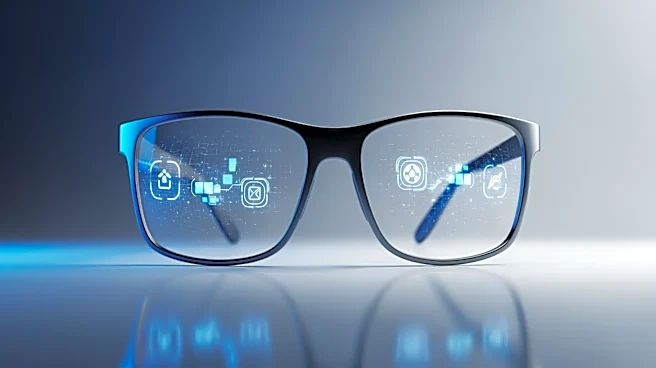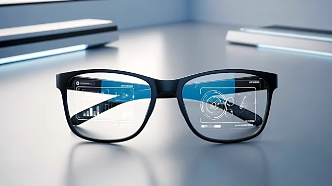
What's Happening?
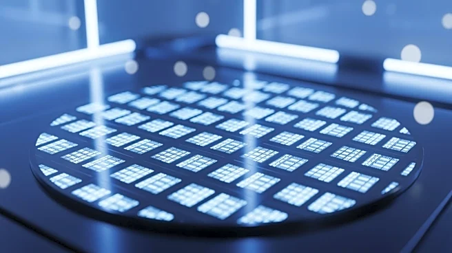
JBD has announced a significant upgrade in its MicroLED microdisplay production, transitioning from a 4-inch to a 12-inch wafer platform. This change enhances manufacturing efficiency and cost-effectiveness,
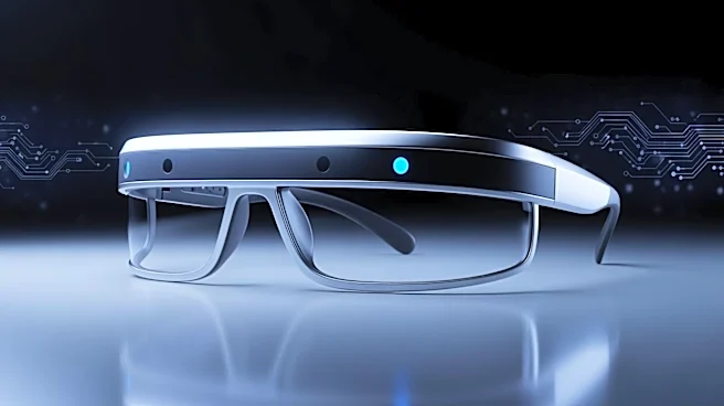
addressing previous limitations in substrate utilization and yield. The new process involves a 'die-to-carrier-to-wafer' bonding scheme, improving the utilization of silicon backplane wafers and reducing defects. This advancement positions JBD to better meet the growing demand for high-performance displays in AR/AI smart glasses and other applications.
Why It's Important?
The shift to 12-inch wafer technology marks a critical step in the evolution of MicroLED manufacturing, enabling more scalable and cost-efficient production. This development could accelerate the adoption of MicroLED displays in various consumer and commercial applications, including augmented reality and automotive displays. By improving yield and reducing costs, JBD's innovation could make high-quality MicroLED displays more accessible, driving growth in the display technology market and potentially leading to new applications and devices.
What's Next?
JBD plans to transfer this new manufacturing architecture to volume production, with end-to-end validation already completed on its pilot line. As the company scales up production, it may explore additional applications for its MicroLED technology, potentially expanding its market presence. The success of this transition could also prompt other companies to adopt similar manufacturing techniques, further advancing the MicroLED industry and its applications.