


What's Happening?
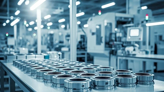
Odisha has inaugurated India's first 3D semiconductor packaging plant in Bhubaneswar, marking a significant step towards technological self-reliance. The facility, supported by both central and state funds, is expected to produce 70,000 glass panels and 50
million assembled units annually. This initiative is part of a broader effort to enhance India's semiconductor manufacturing capabilities, crucial for sectors like AI, defense, and telecommunications. The project is anticipated to create approximately 2,500 jobs, contributing to the local economy and strengthening India's position in the global semiconductor market.
Why It's Important?
The establishment of the semiconductor packaging plant is a strategic move to reduce dependency on foreign technology and enhance India's manufacturing capabilities. This development is crucial for supporting critical sectors and fostering innovation within the country. By boosting local production, the plant is expected to drive economic growth, create job opportunities, and position India as a key player in the global semiconductor industry. The initiative aligns with national goals of technological advancement and economic self-reliance.
What's Next?
The successful operation of the plant could lead to further investments in semiconductor manufacturing and related industries in India. It may also encourage other states to develop similar facilities, contributing to a more robust national semiconductor ecosystem. The project is likely to attract interest from global tech companies looking to invest in India's growing technology sector. Continued support from the government and private sector will be essential to ensure the plant's success and sustainability.