What's Happening?
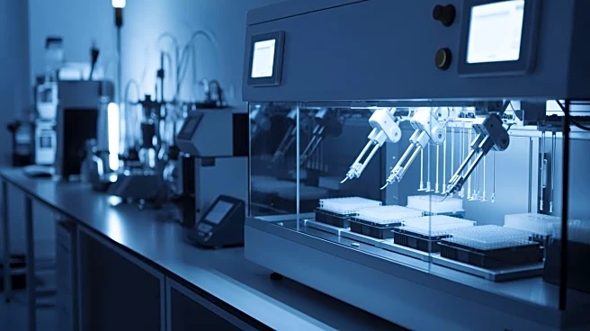
Recent developments in lithography alignment technologies have significantly improved the precision of semiconductor manufacturing. The industry has evolved from basic alignment methods to sophisticated
techniques such as interferometric and heterodyne holographic alignment, achieving nanometre-scale accuracy. This advancement is crucial for integrated circuit manufacturing, where maintaining yield, performance, and reliability in complex, multilayer semiconductor production is essential. The use of bound states in the continuum (BICs), a phenomenon in optics, has been introduced to overcome the optical diffraction limit, a longstanding challenge in alignment technology. BICs allow for the creation of sharp resonances, known as quasi-BIC, which provide new opportunities for precise chip patterning. This method integrates with standard lithography processes, offering a scalable solution compatible with complementary metal–oxide–semiconductor technology.
Why It's Important?
The improvement in lithography alignment technologies is vital for the semiconductor industry, which is foundational to modern electronics. As chip stacking and feature size scaling continue, the demand for greater alignment accuracy grows. This advancement supports the production of more complex and efficient semiconductor devices, which are critical for various applications, including consumer electronics, automotive, and telecommunications. The ability to achieve higher precision in chip manufacturing can lead to better performance and reliability of electronic devices, potentially driving innovation and competitiveness in the U.S. technology sector.