






What's Happening?
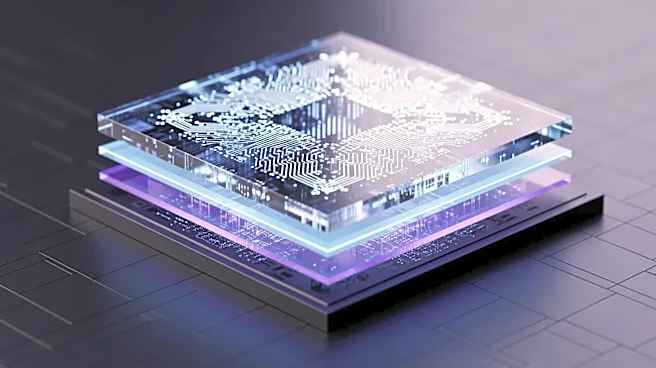
Researchers at the University of Illinois Urbana-Champaign have made significant advancements in monolithic three-dimensional integration of silicon transistors. This innovative approach involves stacking silicon circuits vertically, which increases transistor density
and performance. The team, led by Prof. Qing Cao, has developed a manufacturing process using ultra-thin silicon nanomembranes, allowing for the successful assembly of high-quality layered silicon devices. This method circumvents traditional thermal challenges by employing a low-temperature technique, preserving the integrity of metal wiring. The breakthrough promises faster, smaller, and more energy-efficient computing, crucial for applications in AI and data-centric fields.
Why It's Important?
This development is pivotal for the semiconductor industry, which faces challenges in continuing Moore's Law through traditional scaling methods. By enabling vertical stacking of silicon circuits, the technology offers a sustainable path for increasing transistor density without further miniaturization. This advancement could significantly impact high-performance computing, AI, and machine learning, providing cost savings and enhanced energy efficiency. The research highlights the potential for industrial-scale deployment, supported by partnerships with industry giants like IBM and Intel, positioning the technology as a key player in the future of microprocessor design.
What's Next?
The research team plans to refine and translate their process for adoption in industrial semiconductor foundries. The technology's scalability to more than three layers and compatibility with existing manufacturing processes suggest it could become integral to the evolution of microprocessor design. As the semiconductor industry grapples with the end of traditional scaling, this novel monolithic 3D integration technology stands out as a pragmatic, high-performance solution.
Beyond the Headlines
The implications of this technology extend beyond mere density gains. By reducing wire lengths between devices, it lessens parasitic capacitances and improves communication bandwidth. This opens the door for novel chip designs optimized for heavy computational demands, crucial for sustainable computing progress. The research represents a milestone in materials science innovation, illustrating how interdisciplinary expertise can overcome entrenched technology limits.