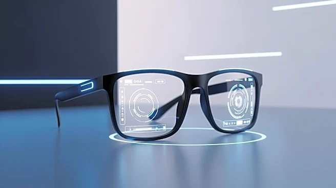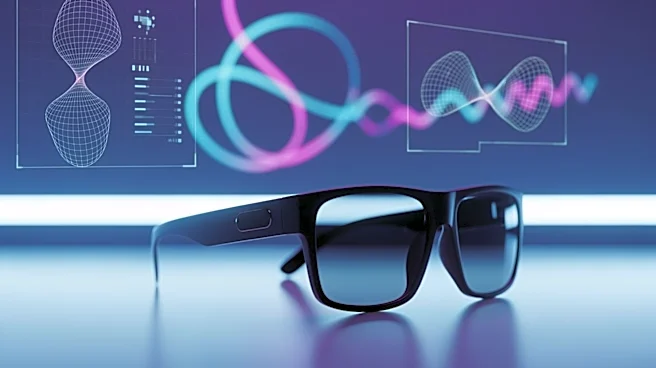
What's Happening?
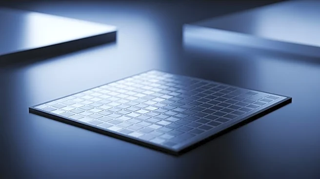
JBD has announced a significant upgrade in its MicroLED microdisplay production by transitioning from a 4-inch to a 12-inch wafer platform. This development marks a major leap in manufacturing efficiency
and cost-effectiveness, addressing long-standing challenges in the industry. The new architecture involves a 'die-to-carrier-to-wafer' bonding scheme, which enhances the utilization of silicon backplane wafers and improves yield by mitigating defects early in the process. This shift is expected to support the growing demand for high-performance displays in AR/AI smart glasses and other applications, as the industry moves towards scalable, cost-efficient production without compromising quality.
Why It's Important?
The transition to a 12-inch wafer platform is crucial for the MicroLED industry as it seeks to meet the increasing demand for advanced displays. By improving manufacturing efficiency and reducing costs, JBD's new platform could accelerate the adoption of MicroLED technology in various sectors, including consumer electronics and automotive industries. This advancement not only enhances JBD's competitive position but also sets a new standard for the industry, potentially leading to broader commercialization of AR smart devices. The improved yield and cost efficiency could make MicroLED displays more accessible, driving innovation and growth in the digital display market.
What's Next?
JBD is now focused on transferring its new 12-inch wafer architecture to volume production, following successful validation on its pilot line. The company aims to leverage this platform to expand its supply capabilities and support the global commercialization of AR smart devices. As the industry continues to evolve, JBD's advancements may prompt other companies to adopt similar technologies, further driving the development of MicroLED displays. The company's commitment to innovation suggests that it will continue to explore new opportunities in the field, potentially leading to further breakthroughs in display technology.
Beyond the Headlines
The shift to a 12-inch wafer platform not only addresses current manufacturing challenges but also positions JBD to explore new applications in 'computing with light.' This could open up opportunities beyond traditional display markets, potentially impacting fields such as optical computing and advanced imaging systems. As pixel pitches shrink and demand for high-precision displays grows, JBD's advancements could influence the broader tech landscape, fostering new collaborations and innovations across industries.