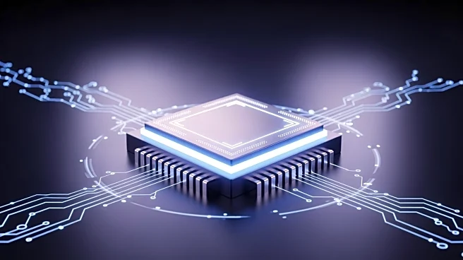

What's Happening?
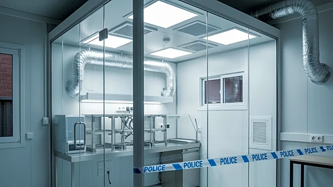
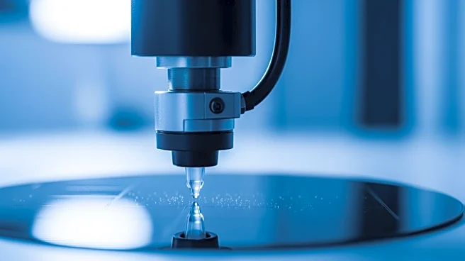
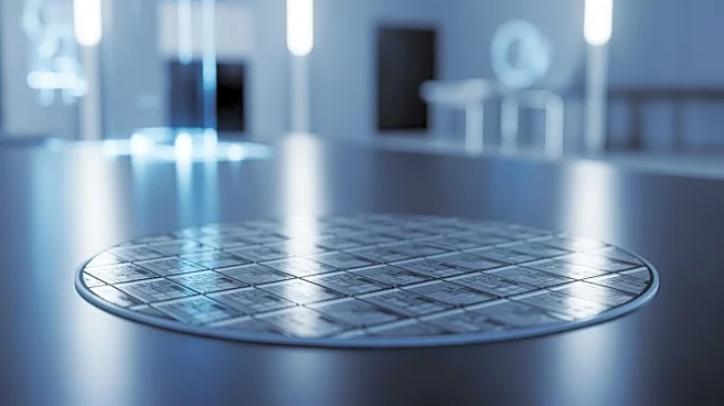
A YouTube channel named Dr.Semiconductor has demonstrated the construction of a semiconductor-class cleanroom inside a wooden shed, using widely available materials. The project involves creating a clean environment necessary for chip manufacturing, typically
found in large factories. The cleanroom is built with insulation, HEPA filters, and epoxy-coated drywall to maintain a particle-free space. The setup includes a 'gowning' area and the cleanroom itself, with positive air pressure maintained to prevent contamination. The cleanroom achieved a Class 100 rating, similar to those used by major chip manufacturers like TSMC and Intel.
Why It's Important?
This development highlights the potential for DIY enthusiasts to engage in complex technological projects, traditionally reserved for large corporations. The ability to create a cleanroom at home could inspire innovation and experimentation in semiconductor manufacturing. However, the cost and complexity of acquiring the necessary chip-making tools remain significant barriers. This project underscores the growing interest in semiconductor technology amid global chip shortages and the AI boom, potentially influencing future educational and hobbyist pursuits in technology.
What's Next?
While the cleanroom itself is a significant achievement, the next steps would involve acquiring the expensive and complex equipment needed for actual chip production. This includes lithography machines and other specialized tools, which are typically beyond the reach of individual hobbyists. The project may inspire further DIY attempts and innovations in semiconductor technology, but large-scale production remains a challenge. The broader implications could include increased interest in semiconductor education and potential small-scale innovations.