








What's Happening?
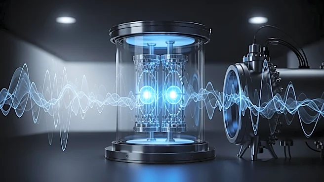
Scientists have created a new compact detector that significantly improves the capture and conversion of terahertz radiation into electrical signals. This advancement utilizes a quantum metasurface, a specially engineered structure that enhances the interaction
between light and matter. The device operates on the in-plane photoelectric effect, where terahertz photons energize electrons within a two-dimensional electron gas, generating an electrical current. Unlike traditional detectors, this method does not require photons to exceed a minimum energy threshold, allowing for more efficient detection. The metasurface concentrates electromagnetic energy into small regions, enhancing the detector's sensitivity and eliminating the need for external optics.
Why It's Important?
This breakthrough in terahertz detection technology has significant implications for various fields, including wireless networks, healthcare, astronomy, and manufacturing quality assurance. The ability to efficiently detect terahertz frequencies could lead to advancements in medical imaging, security scanning, and high-speed communication systems. The integration of the metasurface with semiconductor manufacturing techniques suggests potential for large-scale production and practical deployment. This development bridges the gap between highly sensitive cryogenic detectors and less sensitive room-temperature devices, expanding the range of applications for terahertz technology.
What's Next?
The researchers plan to explore the scalability of the detector design across different frequency ranges, from microwave to mid-infrared wavelengths. Further development could lead to detectors that operate at higher temperatures, making them more accessible for real-world applications. The integration of metasurface optics directly into the detector may simplify packaging and deployment, potentially leading to widespread adoption in various industries. Continued research and optimization could enhance the detector's performance and broaden its applicability.
Beyond the Headlines
The integration of quantum physics and materials engineering in this detector represents a significant step forward in overcoming challenges associated with terahertz technology. The planar architecture of the detector, compatible with standard semiconductor techniques, offers practical benefits for on-chip electronics integration. This innovation could pave the way for new applications in fields that require precise and efficient detection of terahertz frequencies, potentially transforming industries reliant on advanced imaging and communication technologies.