What's Happening?
Researchers at Harvard's School of Engineering have developed a new chip-scale ultraviolet (UV) light source that significantly enhances output power, achieving approximately 120 times more power than
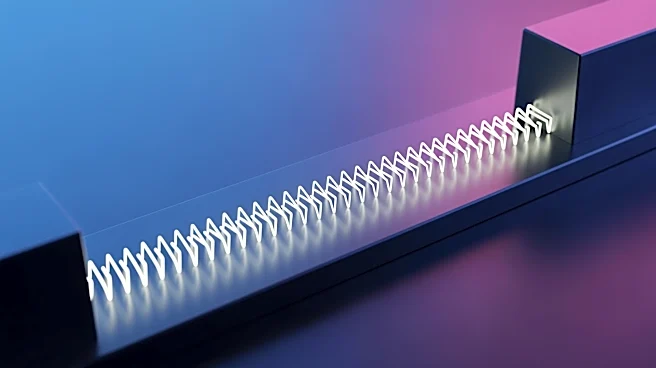
previous designs. The device, which generates 4.2 milliwatts of on-chip UV power at 390 nanometers, marks a significant advancement in photonics research. The breakthrough was made possible through a technique called sidewall poling, which involves placing electrodes directly against the sides of microscopic light-guiding channels on the chip. This method allows for precise reconfiguration of the crystal structure, enhancing light conversion efficiency. The research, published in Nature Communications, highlights the potential applications of this technology in fields such as environmental sensing, quantum computing, and precision optical instrumentation.
Why It's Important?
This development represents a significant leap in the field of photonics, particularly in the generation of UV light at a chip scale. The ability to produce more powerful UV light in a compact form factor opens up new possibilities for various industries. For instance, the technology could lead to advancements in environmental monitoring by enabling more efficient greenhouse gas sensors. Additionally, it could enhance the capabilities of quantum computing hardware and precision optical instruments. The overlap between integrated photonics and lighting technology suggests a future where UV light generation is no longer a limiting factor, potentially leading to innovations in how UV light is packaged and deployed across different sectors.