
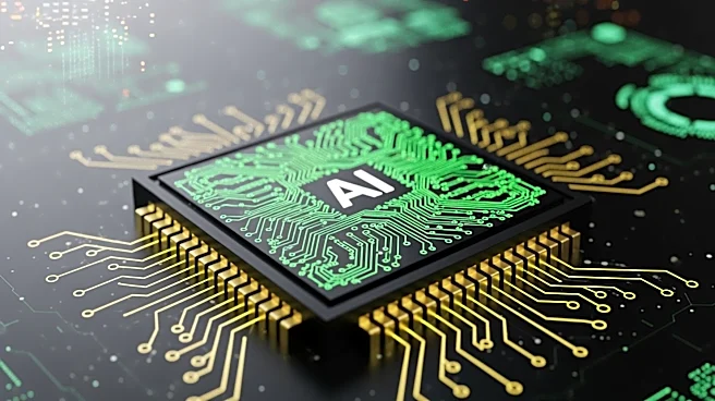

What's Happening?
Bruker Corporation has announced the accelerated development of its photothermal AFM-IR spectroscopy capabilities to address challenges in semiconductor research. The company is expanding the use of AFM-IR technology beyond contamination analysis to support
next-generation semiconductor technologies, including EUV photoresist patterning and advanced materials for transistor scaling. In collaboration with imec, a leading research hub, Bruker has installed its Dimension IconIR system to evaluate the utility of this technology in nanoscale chemical characterization. This collaboration aims to provide insights into material behavior and interfaces that influence semiconductor process development and device performance.
Why It's Important?
The advancement of photothermal AFM-IR technology by Bruker is crucial for the semiconductor industry as device architectures continue to shrink and become more complex. This technology enables precise characterization of complex semiconductor materials, providing chemical insights that are not accessible with conventional techniques. The collaboration with imec highlights the importance of nanoscale chemical analysis in understanding material interactions and improving device concepts. As semiconductor research evolves, the ability to conduct label-free chemical analysis with high resolution is essential for developing next-generation devices, potentially leading to significant advancements in the industry.
What's Next?
Bruker's collaboration with imec is expected to expand the capabilities of photothermal AFM-IR technology in semiconductor research environments. The ongoing evaluation of this technology will likely lead to further insights into material systems and interfaces, enhancing the understanding of semiconductor processes. As the industry continues to face evolving metrology requirements, the adoption of advanced characterization techniques like AFM-IR will be critical. Bruker's continued investment in this area suggests that further developments and applications of this technology are anticipated, potentially influencing future semiconductor research and development.