


What's Happening?
A recent study published in Advanced Photonics introduces a novel approach to enhance the performance of atomically thin semiconductors, such as tungsten disulfide (WS2), which are pivotal for next-generation photonic technologies. These materials, despite
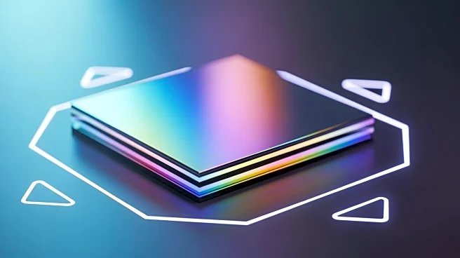
their single-atom thickness, can host tightly bound excitons that interact strongly with light, making them suitable for applications in quantum optics and sensing. The study reveals a strategy that involves placing a single layer of WS2 on nanoscale air cavities, known as Mie voids, within a high-index crystal of bismuth telluride (Bi2Te3). This configuration significantly boosts light emission and nonlinear optical signals, offering new insights into light behavior at small scales. The design allows for enhanced light interaction by confining it within subwavelength air cavities, thus improving the efficiency of light emission and frequency conversion.
Why It's Important?
This development is crucial as it addresses the challenge of weak light emission and inefficient frequency conversion in atomically thin semiconductors due to their minimal material presence. By enhancing the interaction of light with these materials, the new design could lead to significant advancements in the fields of quantum optics and compact on-chip light sources. The ability to boost light emission and nonlinear optical effects without altering the material itself opens up new possibilities for the development of advanced photonic devices. This could have a substantial impact on industries relying on photonic technologies, potentially leading to more efficient and compact devices for various applications.
What's Next?
The study suggests that this new platform could enable further advancements in nonlinear light generation, surface-enhanced sensing, and programmable photonic devices based on two-dimensional semiconductors. The approach of using Mie-void heterostructures could be further explored to enhance other atomically thin materials, potentially leading to a broader range of applications in photonics. Future research may focus on optimizing the design and exploring its applicability to other materials and configurations, paving the way for more efficient and versatile photonic technologies.