




What's Happening?
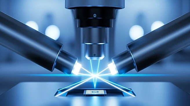
ZEISS has introduced the Crossbeam 750 FIBSEM, a cutting-edge tool designed to improve semiconductor failure analysis. This new technology offers enhanced precision in TEM lamella preparation, tomography, and advanced nanofabrication. The Crossbeam 750 features
a new Gemini 4 SEM objective lens and a next-generation scan generator, providing better resolution and signal-to-noise ratio (SNR). These improvements lead to more detailed imaging and shorter acquisition times, crucial for semiconductor failure analysis. The system's low-kV FIB performance allows for more precise lamella preparation, reducing damage and rework, and accelerating the time to TEM.
Why It's Important?
The introduction of the ZEISS Crossbeam 750 represents a significant advancement in semiconductor failure analysis technology. As the semiconductor industry continues to push the boundaries of miniaturization and complexity, precise and efficient analysis tools are essential. The Crossbeam 750's ability to deliver high-resolution images and reduce sample damage enhances the accuracy and reliability of failure analysis, which is critical for improving yield and reducing production costs. This technology supports faster decision-making and more efficient workflows, enabling semiconductor companies to maintain a competitive edge in a rapidly evolving market.
What's Next?
The adoption of the ZEISS Crossbeam 750 is expected to increase as semiconductor manufacturers seek to enhance their failure analysis capabilities. The tool's advanced features will likely lead to broader applications in materials science and nanofabrication, further driving innovation in these fields. As the demand for semiconductors continues to grow, the need for precise and efficient analysis tools will become even more critical, positioning ZEISS as a key player in the industry.