


What's Happening?
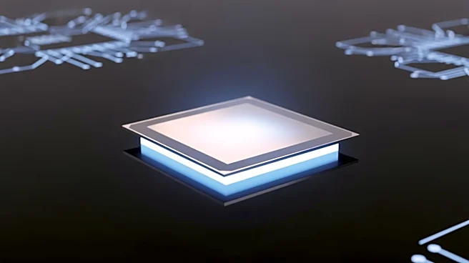
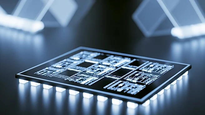
TSMC has introduced its latest A13 process technology at the 2026 North America Technology Symposium in Santa Clara, California. This new process is a direct shrink of the A14 node, offering more compact and efficient designs to meet the growing computational
demands of next-generation artificial intelligence, high-performance computing, and mobile applications. The A13 process provides a 6% area savings from the A14 and is backward compatible, allowing for quick design migration. It is scheduled to enter production in 2029. The symposium also highlighted other technological advancements, including the A12 platform enhancement and the N2U 2nm platform, which are set to enhance AI and HPC applications.
Why It's Important?
The introduction of the A13 process signifies TSMC's ongoing commitment to advancing semiconductor technology, which is crucial for maintaining its leadership in the industry. This development is particularly significant as it addresses the increasing demand for more efficient and powerful computing solutions in AI and HPC sectors. The A13 process's backward compatibility ensures a seamless transition for customers, potentially accelerating the adoption of new technologies. TSMC's advancements could have a substantial impact on the semiconductor market, influencing competitors and driving innovation across various tech industries.
What's Next?
TSMC plans to continue its technological advancements with the A13 process entering production in 2029. The company is also working on expanding its 3DFabric® Advanced Packaging and 3D Silicon Stacking technologies to support AI demand. These developments are expected to provide customers with more options for AI compute scaling. As TSMC progresses, it will likely influence the strategies of other semiconductor companies, potentially leading to increased competition and innovation in the industry.