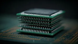


Chip Architecture Evolution
The architecture of computer chips has always strived for greater density, making them more powerful and efficient. Traditionally, engineers have increased
the number of transistors by shrinking their size and placing them closer together. This shrinking process, however, is now reaching its physical limits, creating significant challenges for future advancements. MIT researchers addressed this problem by finding a novel method to stack transistors on top of each other, essentially creating a multi-layered chip architecture. This approach avoids the limitations imposed by shrinking transistors and offers a different path to improve chip performance. This could enable unprecedented computing power without necessarily shrinking transistor sizes further, leading to more compact and powerful devices.
Layering Transistor Advantage
The main benefit of this new method lies in its potential to increase the number of transistors without shrinking their individual size. This is particularly crucial because shrinking transistors further is becoming increasingly difficult and expensive. The ability to layer transistors allows engineers to pack more computational power into a chip. This layered approach enables more complex chip designs and faster processing speeds. By using this technique, manufacturers can maintain or even decrease the chip size while dramatically increasing its processing power. This advance allows for the continued enhancement of computing capabilities at a rate that would otherwise be difficult to achieve, creating possibilities for more sophisticated applications, from high-performance computing to everyday electronics.
Technical Implementation Details
While details of the precise layering methodology are not widely available, the underlying principle involves creating a second layer of transistors on top of the first. This is achieved through innovative materials and manufacturing processes. The researchers likely had to devise techniques for interconnecting these layers, ensuring signals can travel efficiently between them. A key challenge is managing the heat generated by the stacked transistors. It involves careful thermal management strategies to prevent overheating and maintain chip performance. The success of this technique relies heavily on precise alignment and robust inter-layer connections, making it more challenging to implement than current single-layer methods, but also immensely promising in long-term benefits.
Impact on Computing Power
The implications of this technology are far-reaching, with the potential to double the number of transistors. This translates directly to increased computing power. Such a leap would fuel advancements in several sectors, including artificial intelligence, data processing, and high-performance computing. Faster chips enable complex calculations that are currently impossible or incredibly slow, leading to more responsive systems and enhanced efficiency. Furthermore, this innovation could extend the lifespan of Moore's Law, which stated that the number of transistors on a microchip doubles about every two years, thereby pushing the boundaries of technological progress. This could also affect devices such as smartphones and laptops by enabling more powerful processors in smaller formats, enhancing user experiences.
Future Research Pathways
Future research is likely to focus on refining the layering process to optimize performance. Scientists will explore materials to improve efficiency and reduce heat generation. One area of focus involves enhancing the interconnection between the transistor layers, minimizing signal delays, and maximizing bandwidth. Manufacturing methods will need to be scaled up to meet industrial standards, facilitating widespread adoption. Researchers will also explore new chip designs to fully utilize the enhanced architecture enabled by this new approach. This could involve creating customized chip architectures to suit various application domains, ranging from specialized AI accelerators to energy-efficient embedded systems. These efforts can help integrate this technology into mainstream chip manufacturing.