


A New Era Begins
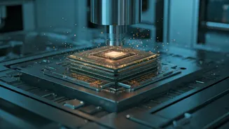
The Indian government has officially sanctioned the creation of the country's very first advanced 3D chip packaging plant, a monumental step forward designed
to bolster India's burgeoning semiconductor capabilities. This state-of-the-art facility, set to be developed by a prominent US-based entity through its Indian subsidiary, is slated to commence operations by 2025. This development signifies a critical advancement in India's strategic ambition to emerge as a global leader in both semiconductor manufacturing and design. The plant will specialize in cutting-edge packaging techniques, which are vital for optimizing the performance and energy efficiency of microchips. Such an initiative is projected to generate a substantial number of employment opportunities and attract considerable further investment into this high-technology sector. The government's proactive Production Linked Incentive (PLI) scheme for semiconductors has been instrumental in attracting these significant investments, underscoring India's increasing prowess in advanced manufacturing.
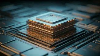
Decoding 3D Glass Technology
At its core, 3D glass semiconductor technology represents a sophisticated evolution in chip processing. This advanced method leverages specialized glass substrates, enabling the intricate, three-dimensional arrangement of electrical components. Unlike the conventional silicon used in most chips, glass offers distinct advantages, particularly in radio frequency applications where it exhibits superior performance. It also boasts lower electrical signal loss and enhanced thermal stability, making it ideal for integrating passive electronic components. The facility established in Bhubaneswar will be responsible for the crucial assembly and packaging of these advanced chips, integrating them into functional units that drive modern electronic devices. This technological leap is a key component in enhancing the efficiency and capability of semiconductors.
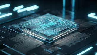
Semiconductors: The Digital Backbone
Semiconductors, often referred to as microchips, are the fundamental building blocks of virtually all modern electronic devices. These integrated circuits are intricate networks of transistors, diodes, capacitors, and resistors etched onto a wafer, typically made of silicon. Semiconductors occupy a unique position in electrical conductivity, falling between conductive materials like copper, which allow free electron flow, and insulators like glass, which impede it. In their pure, natural state, semiconductors are poor conductors. However, their conductivity can be precisely controlled by introducing specific impurities, a process known as doping. For instance, adding phosphorus to silicon or germanium allows for the controlled flow of negative charge carriers, creating n-type semiconductors. This ability to control electrical flow is what makes them indispensable for processing, storing, and transmitting data, powering everything from smartphones and computers to advanced medical equipment and critical infrastructure.
India's Strategic Push
The establishment of the 3D chip packaging plant is part of a broader, concerted effort by the Indian government to cultivate a robust domestic semiconductor ecosystem. Spearheaded by initiatives like the India Semiconductor Mission (ISM), launched in 2021, the nation aims to foster self-reliance in semiconductor design and manufacturing. The ISM, operating under the Ministry of Electronics and Information Technology (MeitY), provides a strategic framework to drive innovation, create employment, and stimulate economic growth within the sector. Complementing this is the Semicon India Programme, which offers financial incentives to companies investing in various facets of the semiconductor industry, including fabrication plants, display manufacturing, and assembly, testing, marking, and packaging (ATMP) facilities. The programme includes specific schemes like the Design Linked Incentive (DLI) Scheme, which supports chip design startups and research and development efforts. A significant milestone in this journey was the unveiling of Vikram 3201, India's first indigenous microprocessor developed by ISRO's Semiconductor Laboratory, showcasing the nation's growing design capabilities and its drive towards strategic electronic self-sufficiency.