





Musk's Mega Chip Ambition
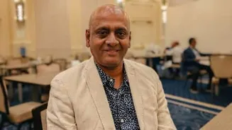
Christophe Fouquet, the chief executive of ASML, has shared significant details about his direct discussions with Elon Musk concerning the highly ambitious
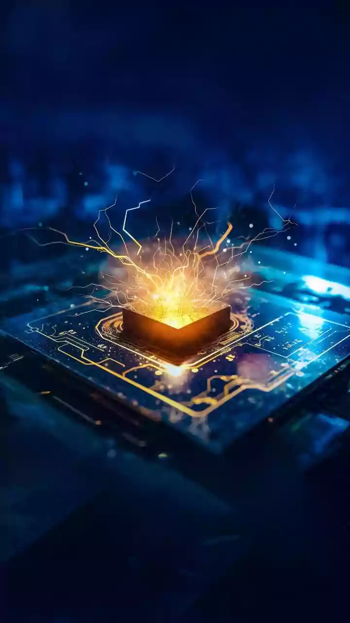
TeraFab semiconductor initiative. Fouquet emphasized that Musk's commitment to establishing one of the largest chip manufacturing facilities ever conceived is profound. He described Musk as "very serious" about the project, which was first unveiled in March with an initial investment of $20 billion. The TeraFab project aims to consolidate the production of logic chips, memory, and advanced packaging solutions under a single operational umbrella in Texas. This groundbreaking venture has already attracted major industry players, with Intel joining in April to contribute its advanced 14A process technology. Furthermore, SpaceX has initiated plans for a colossal semiconductor facility in Grimes County, Texas, projecting potential expansion costs that could reach an astonishing $119 billion, underscoring the sheer scale of Musk's vision in reshaping the semiconductor landscape.
AI Drives Chip Shortage
The global semiconductor industry is poised to face a significant capacity crunch in the coming years, a challenge exacerbated by the insatiable demand for artificial intelligence technologies. ASML's CEO, Christophe Fouquet, highlighted this critical issue during a recent tech event. He warned that the rapid proliferation of AI applications worldwide is placing immense pressure on existing manufacturing capabilities and equipment suppliers. Projects like TeraFab, alongside other significant endeavors such as Starlink, will undoubtedly contribute to this strain by requiring substantial volumes of advanced semiconductor manufacturing equipment. As the sole global provider of the indispensable EUV lithography systems, ASML finds itself at the nexus of this burgeoning demand. Any new entrant into advanced chipmaking, including the ambitious TeraFab, will necessitate multi-billion dollar investments in ASML's cutting-edge machinery to achieve their manufacturing goals. The company currently holds substantial orders from virtually every major player in the foundry and memory sectors, including prominent names like TSMC, Samsung, SK Hynix, Micron, and Intel, reflecting its pivotal role in the future of chip production.
Next-Gen Lithography Arrives
The arrival of the next generation of logic chips, manufactured using ASML's groundbreaking High NA EUV lithography systems, is imminent, with the first outputs expected within mere months. Intel stands as the pioneer in adopting this advanced technology, having successfully completed acceptance testing of its Twinscan EXE:5200B system at its D1X fab in Oregon by the end of last year. These sophisticated High NA tools distinguish themselves through their 0.55 numerical aperture lens, a technological leap that enables a remarkable increase in transistor density, approximately 2.9 times that of current EUV systems, all within a single exposure process. This advancement signifies a crucial step forward in miniaturization and performance for semiconductor devices. Beyond lithography, ASML is also actively expanding its product portfolio by developing a second advanced packaging tool. While Fouquet acknowledged this segment is currently a smaller component of ASML's business, he expressed optimism about the new opportunities it presents for the company's future growth and market diversification within the semiconductor ecosystem.
Export Controls Debate
In recent discussions, ASML's CEO, Christophe Fouquet, has voiced his reservations regarding proposed export controls, specifically those recently introduced by U.S. lawmakers that could restrict the sale and servicing of ASML's DUV lithography tools to Chinese customers. Fouquet pointed out that the DUV immersion systems currently supplied to China are based on technology that first emerged in 2015, placing them significantly behind the cutting edge of semiconductor manufacturing. He argued that imposing further restrictions could inadvertently accelerate China's domestic efforts to develop its own competing technologies. Using a vivid analogy, Fouquet explained that enforcing such limitations is akin to placing someone in a desert and forbidding access to food, suggesting it would ultimately spur innovation out of necessity. He believes that such actions might only hasten China's drive for self-sufficiency in semiconductor tool development, rather than effectively hindering its progress in the long term, framing it as a matter of survival for technological advancement.