


Extreme Environment Solutions
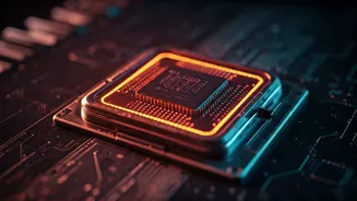
Researchers at the National Institute of Standards and Technology (NIST) have pioneered an innovative approach to packaging photonic chips, significantly
enhancing their resilience in extreme environmental conditions. This breakthrough is poised to unlock the potential of photonic chip-based technologies in a variety of challenging settings. Imagine probes venturing into the vastness of deep space, instruments operating within the intense heat and radiation of nuclear reactors, or sensitive equipment functioning in the near-absolute vacuum of space or at temperatures approaching absolute zero. The developed packaging technique makes these scenarios feasible. Nikolai Klimov, the lead physicist on the project at NIST, indicated that the adoption of this new packaging method by some chip manufacturers could occur within the next one to two years. This adoption is anticipated in specialized sectors that have an urgent need for photonics capable of withstanding extreme conditions, such as quantum cryogenic systems, advanced nuclear instrumentation, and hardware destined for space exploration. This development signifies a major leap forward in expanding the operational capabilities of photonic technologies into previously inaccessible domains.
Bridging the Packaging Gap
The escalating demand for sophisticated semiconductors is driving the expansion of chip fabrication facilities. Consequently, there's a growing desire among manufacturers to integrate photonic chips into a broader range of applications. However, the critical challenge hindering this widespread adoption has been effective packaging. In the realm of chip manufacturing, 'packaging' refers to the essential protective casing and intricate connection system that encloses a chip. This system is vital for linking the chip to the external world, facilitating communication through optical fibers, electrical contacts, and other necessary components. Robust packaging ensures that chips can be integrated into compact and dependable devices without succumbing to damage or misalignment. NIST highlights that proper packaging is fundamental to the practical usability and longevity of advanced microelectronic and optoelectronic devices, particularly as they are miniaturized and deployed in increasingly complex systems.
Photonic Advantages Over Silicon
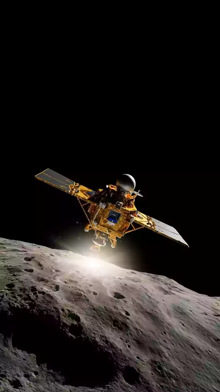
Photonic integrated chips offer compelling advantages over traditional silicon-based alternatives, primarily in their ability to transmit data at remarkably high speeds while consuming significantly less power. These characteristics have already positioned them as central components in critical fields such as telecommunications, sophisticated medical diagnostics, and advanced sensing technologies. Despite these benefits, their utility in more demanding or hazardous environments has been limited. This limitation stems from the inability of conventional packaging methods to maintain stable optical connections when subjected to factors like intense radiation, extreme temperature fluctuations (both high and low), or ultrahigh vacuum conditions. Such adverse environments are prevalent in many areas where photonic integrated chips could offer substantial improvements, including the development of powerful quantum computing platforms, the rigors of space missions, the core of nuclear reactors, the high-energy particle accelerators used in research, and various industrial and energy-related applications.
Novel Bonding Technique
To enable photonic integrated chips to perform reliably in these challenging operational settings, NIST researchers focused on developing a novel method for securely attaching optical fibers to the chips. Traditional adhesives, such as organic polymer glues, have proven inadequate because they tend to crack, release gases (outgas), or degrade when exposed to extreme cold, intense radiation, vacuums, or high temperatures. When these adhesive failures occur, the photonic chip can no longer function as intended, rendering the device inoperable. The NIST scientists ingeniously adapted a technique known as hydroxide catalysis bonding. This process creates an inorganic, glass-like chemical bond directly between the optical fiber and the photonic chip, bypassing the need for conventional glues. Instead, the method utilizes a minuscule amount of sodium hydroxide solution to molecularly fuse the surfaces together, resulting in a connection that is both rigid and exceptionally stable, thus overcoming the limitations of traditional bonding agents.
Future Prospects and Adoption
This significant advancement represents a major stride towards integrating the speed and energy efficiency of photonics into environments where conventional semiconductor chips and traditionally packaged photonic chips have been unable to operate effectively. Looking ahead, the widespread adoption of this technology in mainstream manufacturing hinges on further developments aimed at reducing costs and accelerating production processes. Several avenues exist for achieving these goals, including substantially shortening the current curing time, which presently takes approximately a week but could be reduced to mere hours or even less. Furthermore, scaling up the production capabilities and rigorously demonstrating long-term reliability across a diverse range of devices will be crucial. Klimov anticipates that with these concentrated efforts on further technological development, broader commercial adoption could materialize within a three to five-year timeframe, or potentially sooner, depending on the intensity of investment and research dedicated to this promising field.