


Foundation Stone Laid
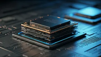
In a pivotal moment for India's technological aspirations, Bhubaneswar has become the site of the nation's first advanced 3D semiconductor packaging unit.
The foundation stone for this cutting-edge facility was jointly laid by Odisha Chief Minister Mohan Charan Majhi and Union IT Minister Ashwini Vaishnaw. This significant undertaking represents a substantial step towards enhancing India's indigenous capabilities in the semiconductor manufacturing sector. The project is being brought to life by the US-based 3D Glass Solutions Inc. through its Indian subsidiary, Heterogeneous Integration Packaging Solutions Pvt Ltd (HIPSPL), establishing a vertically integrated, advanced packaging and embedded glass substrate ATMP facility within Info Valley in the Khordha district.
Economic Impact and Output
The establishment of this advanced facility entails a total investment of Rs 1,943.53 crore, supported by Rs 799 crore in central fiscal aid and an additional Rs 399.5 crore from the state. Upon full operationalization, the unit is projected to achieve remarkable production figures, including an annual output of 70,000 glass panels, 50 million assembled units, and approximately 13,000 advanced 3D Heterogeneous Integration (3DHI) modules. Beyond its manufacturing prowess, the project is set to be a significant job creator, expected to generate around 2,500 direct and indirect employment opportunities, thereby contributing substantially to the local economy and providing a boost to the region's workforce.
Strategic Sectoral Contributions
The chips manufactured at this state-of-the-art facility in Odisha are slated to serve a range of crucial and high-growth sectors. These include pivotal industries such as aerospace, defence, artificial intelligence (AI), 5G technologies, and Data Centres. Minister Vaishnaw emphasized that this project is among the most advanced manufacturing initiatives in the country, designed to significantly fortify India's entire semiconductor value chain. Chief Minister Majhi echoed this sentiment, describing the unit as a historic milestone that brings immense pride to Odisha and the nation, positioning India for greater self-reliance in critical technological domains.
Transforming Odisha's Economy
This venture is poised to transform Odisha's industrial profile, traditionally known for its mineral and metal resources, into a hub for advanced technology and innovation. The initiative directly aligns with Prime Minister Narendra Modi's vision of making India self-sufficient in semiconductor and electronics manufacturing. The burgeoning semiconductor ecosystem in Odisha is expected to create abundant employment prospects for engineering graduates, diploma holders, and ITI students, fostering a shift from a resource-based economy to one driven by technological advancements and high-value manufacturing. This strategic move signifies Odisha's readiness to play a leading role in the nation's technological advancement.
National Semiconductor Progress
The Union Minister highlighted the impressive growth trajectory of India's electronics manufacturing sector, noting a sixfold increase in production over the past 12 years. This progress has elevated India to become the world's second-largest mobile phone manufacturer and a leading exporter. The inauguration of the 3D chip packaging unit is part of a larger strategy, with two semiconductor projects already approved for Odisha under the India Semiconductor Mission, and three more electronics and semiconductor-related proposals in the pipeline. Discussions are also underway with global industry giants like Intel for potential future investments in the state, underscoring India's growing appeal in the global semiconductor landscape.