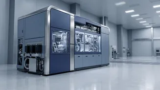







The Most Expensive Tool on Earth
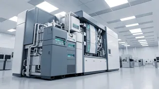
Meet the High-NA EUV lithography system, built by the Dutch company ASML. It is, by a wide margin, one of the most complex and expensive manufacturing tools ever created. The world’s leading chipmakers, including Intel, Samsung, and TSMC, are all staking
their futures on this technology. Intel, an early adopter, has already begun using the machine for high-volume manufacturing of some of its latest processors. Following suit, Samsung and SK Hynix plan to integrate these systems into their production lines by 2028, with TSMC targeting 2030 for its most advanced chips. The demand, fueled by the explosive growth of artificial intelligence, is so intense that ASML's order books are nearly full for years to come.
ASML: The Monopoly Nobody Knows
While names like Intel and Samsung are household brands, ASML operates in relative obscurity, yet holds a position of immense power. Headquartered in Veldhoven, Netherlands, the company has a complete monopoly on the production of Extreme Ultraviolet (EUV) lithography machines, the only technology capable of producing the most advanced chips. This dominance wasn't accidental. It's the result of decades of research and billions in investment to solve one of physics' most difficult challenges: how to print circuits just a few atoms wide. Competing firms in Japan and China produce older-generation equipment, but they remain years, if not decades, behind ASML's cutting-edge EUV technology.
How to Print with Light
At its core, lithography is like a highly advanced form of photography. To create a chip, circuit patterns are projected from a stencil, known as a photomask, onto a silicon wafer coated with light-sensitive material. For decades, this was done with Deep Ultraviolet (DUV) light. But as transistors shrank to sizes smaller than a virus, a new approach was needed. ASML's breakthrough was to harness Extreme Ultraviolet (EUV) light, which has a wavelength of just 13.5 nanometers—almost in the X-ray range. Creating this light is a monumental feat: a powerful laser zaps tiny droplets of molten tin 50,000 times a second, creating a plasma that emits EUV radiation. This light is then focused by a series of mirrors so perfectly polished that if one were scaled to the size of Germany, the largest bump would be less than a millimeter high.
The Jump to High-NA
The new $400 million machine represents the next generation of this technology, known as High-NA (High Numerical Aperture). In simple terms, its more advanced optical system can collect light from a wider angle, allowing it to print even finer details. While the previous generation of EUV machines could print features down to 13 nanometers, the new High-NA systems can achieve a resolution of 8 nanometers. This leap is crucial for producing chips at the 2-nanometer node and beyond, continuing the trend described by Moore's Law, which predicts the doubling of transistors on a chip every two years. For chipmakers, using a single High-NA exposure can replace multiple complex steps required with older machines, potentially saving time, reducing costs, and improving the quality of the final product.
The Future of Technology on a Wafer
This isn't just an abstract technological race. The chips made with these machines will power everything from the next generation of smartphones and AI data centers to advanced medical devices and autonomous vehicles. The immense cost and complexity mean only a handful of companies can afford to play at this level, and they all depend on ASML. Recognizing this shared dependency, rivals like Intel, Samsung, and TSMC have even begun collaborating with ASML on developing future standards, such as larger photomasks, to make the manufacturing process more efficient. This underscores the reality of the modern semiconductor industry: progress is no longer just about competition, but also about the coordinated effort required to push the boundaries of science and engineering.